A high-efficiency white light organic electroluminescent device
An electroluminescent device, organic technology, applied in the direction of electric solid devices, electrical components, luminescent materials, etc., can solve the problems of triplet energy level mismatch and low luminous efficiency.
- Summary
- Abstract
- Description
- Claims
- Application Information
AI Technical Summary
Problems solved by technology
Method used
Image
Examples
Embodiment 1
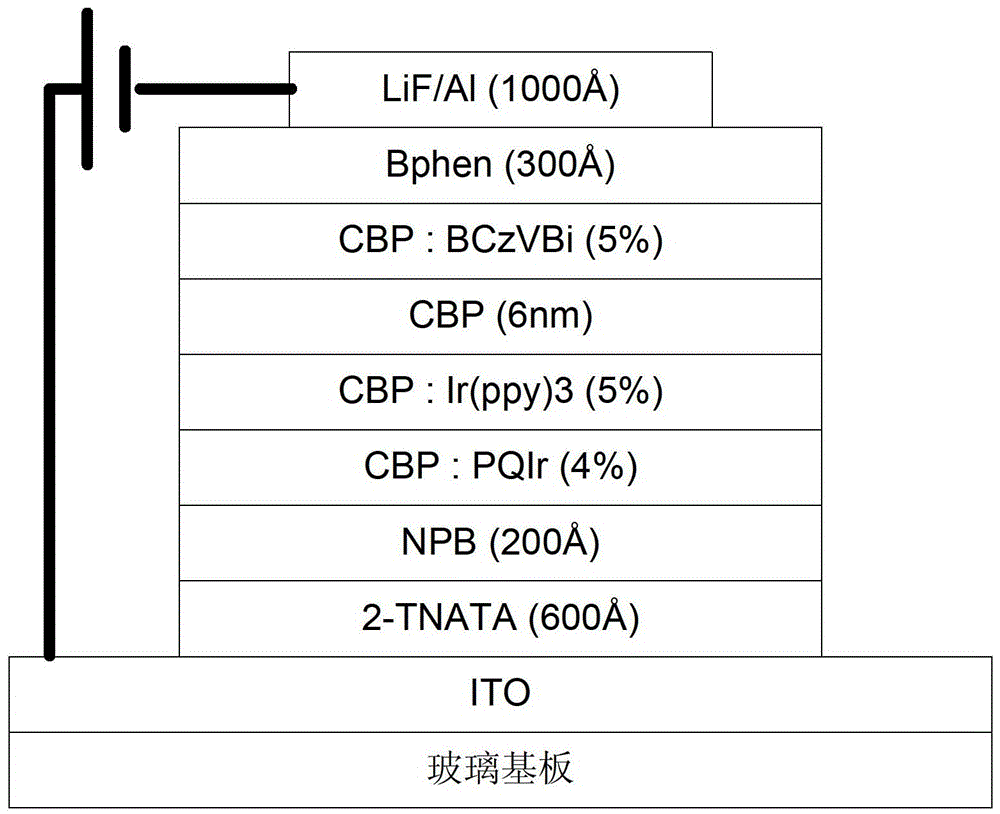
[0144] The device structure of this embodiment is as follows:
[0145] HAT / MTDATA / HAT / NPB / HTL-2:Ir(MDQ) 2 (acac) / HTL-2:ET-2:Ir(ppy) 3 / HTL-2:ET-2 / ADN:BD-1 / ETL-1 / LiF / Al
[0146] This embodiment provides a white light OLED device with three light-emitting centers. The three light-emitting layers are red, green, and blue in turn. The red phosphorescent light-emitting layer uses the compound shown in the formula HTL-2 as the host material, and Ir(MDQ) 2 (acac) as a dye; the main material of the green phosphorescent light-emitting layer is a mixture of two materials, which are the compound shown in formula HTL-2 and the bis(9,9'-spirobifluoren-2-yl) shown in formula ET-2 ketone), the dye is Ir(ppy) 3 ; The barrier layer is a compound shown in formula HTL-2, a mixture of bis (9,9'-spirobifluoren-2-yl) ketone shown in ET-2); the main material of the blue fluorescent light-emitting layer is ADN, and the dye is the formula The compound shown in BD-1; the electron transport materia...
Embodiment 2
[0157] The device structure and preparation method of Examples 2-5 are basically the same as those of Example 1, except that in step ⑥, in Example 2, the compound shown in formula HTL-2 is doped with a compound shown in formula ET-2. The evaporation thickness is 5nm, wherein the compound represented by the hole transport material formula HTL-2 accounts for 35wt% of the barrier layer, and the compound represented by the electron transport material formula ET-2 accounts for 65wt% of the barrier layer.
Embodiment 3
[0158] In Example 3, the compound shown in the formula HTL-2 doped with the compound shown in the formula ET-2 has an evaporation thickness of 5nm, wherein the compound shown in the hole transport material formula HTL-2 accounts for 15wt% of the barrier layer, and the electron transport material formula The compound shown in ET-2 accounts for 85wt% of the barrier layer.
PUM
| Property | Measurement | Unit |
|---|---|---|
| thickness | aaaaa | aaaaa |
| thickness | aaaaa | aaaaa |
| thickness | aaaaa | aaaaa |
Abstract
Description
Claims
Application Information


