Band gap reconfigurable micro-band ultra wide band filter

An ultra-wideband filter and microstrip technology, applied in waveguide devices, electrical components, circuits, etc., can solve the problems of large insertion loss, wide bandgap bandwidth, and large passband insertion loss, etc., to achieve reconfigurable dual Bandgap response, effect of improving band utilization

Active Publication Date: 2013-07-10
陕西锦图信息技术有限公司
View PDF4 Cites 11 Cited by
  • Summary
  • Abstract
  • Description
  • Claims
  • Application Information

AI Technical Summary

Problems solved by technology

[0003] In September 2008, Y.H.Chun et al. published "Switchable Embedded Notch Structure for UWB Bandpass Filter" in IEEE Microwave and Wireless Components Letters (vol.18, no.9, pp.590-592, 2008), and proposed a An optional embedded bandgap ultra-wideband filter, which can selectively embed a bandgap in the ultra-wideband passband, but the bandwidth of the bandgap is wide, the ultra-wideband is not flat, and the insertion loss is relatively large; In August 2010, Song Kaijun et al. published "Compact Ultra-Wideband (UWB) Bandpass Filters With Multiple Notched Bands", a new type of dual-bandgap ultra-wideband filter is proposed, which realizes two fixed-frequency bandgaps, that is, the two bandgaps are not reconfigurable, and its bandwidth is wide, and the passband insertion loss is large

Method used


Image

  • Band gap reconfigurable micro-band ultra wide band filter
  • Band gap reconfigurable micro-band ultra wide band filter
  • Band gap reconfigurable micro-band ultra wide band filter

Examples


Embodiment 1

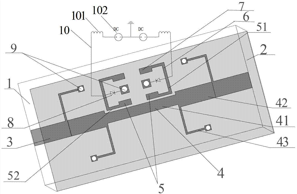
[0052] refer to figure 1 with 2 , the present invention is mainly composed of a microstrip dielectric substrate 1, a metal ground plate 2, a pair of input and output microstrip feeders 3, a microstrip resonator 4, a bandgap resonator 5, a PIN tube 8 and a DC bias circuit 10, wherein:

[0053] The microstrip dielectric substrate 1 adopts a single-sided copper-clad dielectric substrate with a dielectric constant of 2.65 and a thickness of 1mm;

[0054] The metal ground plate 2 is arranged on the lower surface of the microstrip dielectric substrate 1, and the metal ground plate 2 is provided with a ground hole 9;

[0055] The microstrip resonator 4 is arranged on the upper surface of the microstrip dielectric substrate 1, and consists of a half-wavelength microstrip line 41, a quarter-wavelength microstrip line 42 and two groups of center-symmetrical "L"-shaped short-circuit stubs 43, wherein , the half-wavelength microstrip line 41 is connected in series with the quarter-wavel...

Embodiment 2

[0063] The structure of this example is identical with embodiment 1, and the parameter value design different from embodiment 1 is as follows:

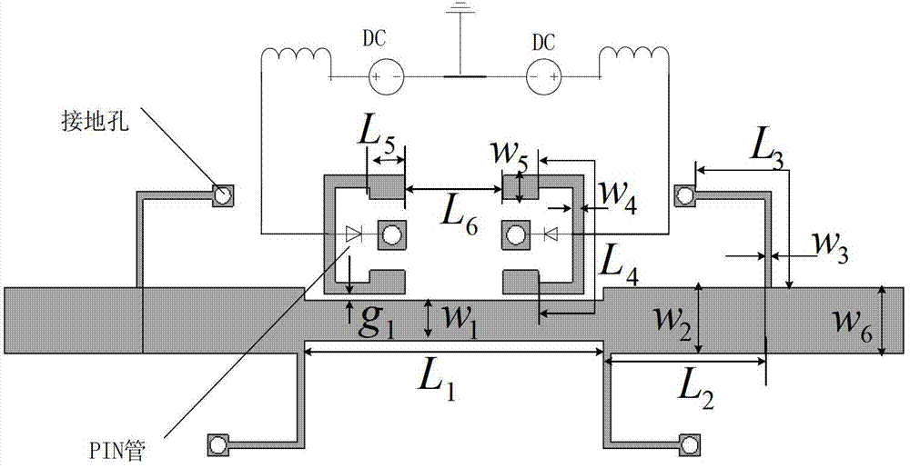
[0064] Bandgap resonator 5 is made up of two symmetrical ladder impedance resonators 51 and 52, and PIN tube 8, wherein, each ladder impedance resonator is made up of high-impedance line 6 and low-impedance line 7, and in the ladder impedance resonator The length L of the high impedance line 6 4 =5.6mm, width w 4 =0.3mm, low impedance line 7 length L 5 =3.0mm, width w 5 =1.0mm, the corresponding resonant frequency f' 0 =8.0GHz, the distance L between the two stepped impedance resonators 51 and 52 6 =5.4mm.

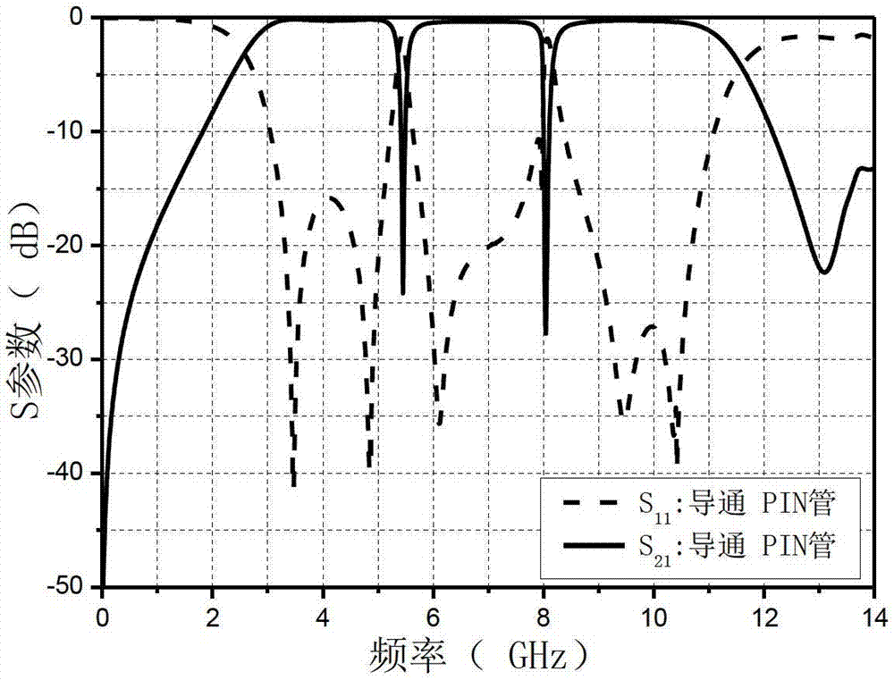
[0065] The frequency response curve of this embodiment is as Figure 5 with 6 shown by Figure 5 It can be seen that when the PIN tube is turned on, the center frequency of the first bandgap is 5.2GHz, the insertion loss is greater than 26dB, the 3dB bandwidth is about 0.15GHz, the center frequency of the second bandgap is...

Embodiment 3

[0067] The structure of this example is identical with embodiment 1, and the parameter value design different from embodiment 1 is as follows:

[0068] Bandgap resonator 5 is made up of two symmetrical ladder impedance resonators 51 and 52, and PIN tube 8, wherein, each ladder impedance resonator is made up of high-impedance line 6 and low-impedance line 7, and in the ladder impedance resonator The length L of the high impedance line 6 4 =5.6mm, width w 4 =0.4mm, low impedance line 7 length L 5 =3.2mm, width w 5 =1.0mm, the corresponding resonant frequency f' 0 =8.0GHz, the distance L between the two stepped impedance resonators 51 and 52 6 =4.8mm.

[0069] The frequency response curve of this embodiment is as follows Figure 7 with 8 shown by Figure 7 It can be seen that when the PIN tube is turned on, the center frequency of the first bandgap is 5.1GHz, the insertion loss is greater than 25dB, the 3dB bandwidth is about 0.15GHz, the center frequency of the second ba...


PUM


Abstract

The invention discloses a band gap reconfigurable micro-band ultra wide band filter which mainly solves the problems that an ultra wide band in-band is uneven, a single-double band gap is reconfigurable, the band gap width is large, and insertion loss is large. The filter comprises a micro-band medium substrate (1), a pair of input-output micro-band feeder lines (3), a micro-band resonator (4), a band gap resonator (5) and a direct current biasing circuit (10). The band gap resonator (5) is arranged on the micro resonator (3) and is formed by two symmetrically-arranged stepped impedance resonators (51, 52) and a PIN tube (8). Each stepped impedance resonator is formed by a high impendence line (6) and a low impendence line (7). The direct current biasing circuit (10) provides variable voltage for the PIN tube (8), and achieves single-double band gap reconfiguration. The band gap reconfigurable micro-band ultra wide band filter can reduce pass band insertion loss, shorten band gap band width, achieve ultra wide band filter characteristics that a first band gap is capable of being switched on and switched off, and a second band gap is not changed and can be used for a wireless communication system.

Description

technical field [0001] The invention belongs to the technical field of electronic devices, in particular to a bandgap reconfigurable microstrip ultra-wideband filter, which can be used for a radio frequency front end of an ultra-wideband wireless communication system. Background technique [0002] In recent years, in wireless communication systems, ultra-wideband UWB technology has attracted more and more attention due to its high data transmission rate, and ultra-wideband filters that meet application needs have become a research hotspot in this field. Ultra-wideband technology requires the use of a very wide radio spectrum, but the spectrum is full of many undesirable narrow-band signals, such as WLAN systems with a frequency range of 5.2GHz to 5.8GHz, satellite communication systems with a frequency of 8.0GHz, these radio signals may interfere UWB system communications. Therefore, a narrow suppression bandgap for electrical switching is introduced in the passband of the ...

Claims


Application Information

Patent Timeline
Patent Type & Authority Applications(China)
IPC IPC(8): H01P1/203
Inventor 吴边张小艳张灵芝邱枫
Owner 陕西锦图信息技术有限公司
Why Eureka
Try Eureka