Creating Anisotropic Diffused Junctions in Field Effect Transistor Devices

A field-effect transistor, transistor technology, applied in semiconductor devices, electrical solid-state devices, semiconductor/solid-state device manufacturing, etc., can solve problems such as degradation of scaling device performance, device performance degradation, etc.

Inactive Publication Date: 2016-01-20
GLOBALFOUNDRIES INC
View PDF7 Cites 0 Cited by
  • Summary
  • Abstract
  • Description
  • Claims
  • Application Information

AI Technical Summary

Problems solved by technology

However, in sub-90nm technology nodes, where S / D stress-inducing elements such as epitaxially grown silicon germanium (eSiGe) and silicon carbide (eSiC) are incorporated for carrier mobility enhancement, the impact on S / D junction depth Scaling degrades device performance due to stress losses
In addition, shallow junctions lead to higher S / D series resistance, further degrading the performance of scaling devices

Method used


Image

  • Creating Anisotropic Diffused Junctions in Field Effect Transistor Devices
  • Creating Anisotropic Diffused Junctions in Field Effect Transistor Devices
  • Creating Anisotropic Diffused Junctions in Field Effect Transistor Devices

Examples


Embodiment Construction

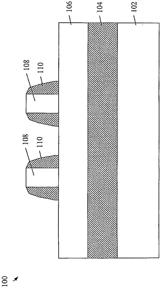
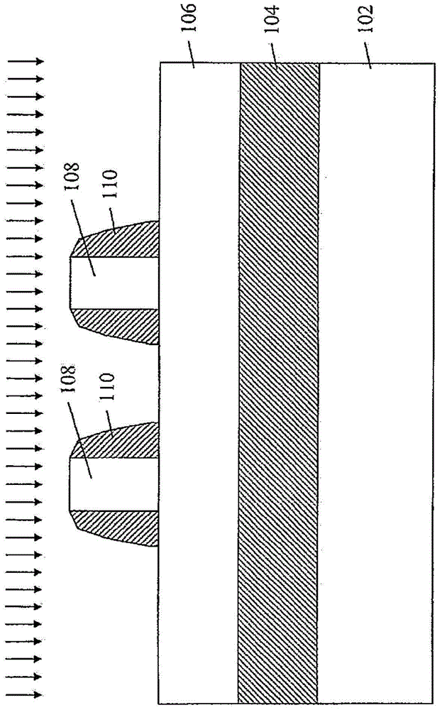
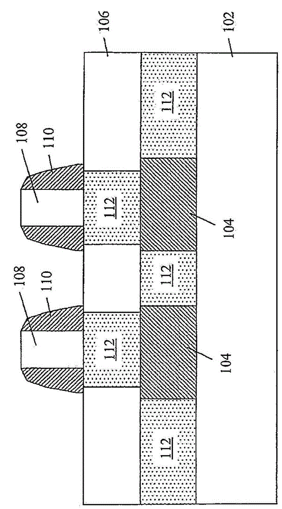
[0023] Disclosed herein are methods and structures for creating anisotropically diffused junctions in field effect transistor (FET) devices. In particular, embodiments of methods for promoting vertical diffusion of NFET and / or PFETS / D junctions while suppressing lateral diffusion are disclosed, which embodiments enable the realization of deep source / drain. Thus, such a process reduces the S / D series resistance of NFETs and / or PFETs and enables the use of thicker silicon-on-insulator (SOI) substrates, which is useful for eSiGep-type FETs (PFETs) and eSiCn-type FETs (NFETs) The stress optimization of is advantageous. In the following description, the boron difluoride (BF2) dopant in the PFET device is equivalent to the arsenic (As) dopant in the NFET device, while the boron (B) dopant in the PFET device is equivalent to the NFET device Phosphorus (P) dopant in .

[0024] In the embodiments shown below, exemplary NFET devices are shown. However, it should be understood that t...


PUM


Abstract

A method for forming a transistor device comprising implanting a diffusion-inhibiting species in a semiconductor-on-insulator substrate, the semiconductor-on-insulator substrate comprising a bulk substrate, a buried insulator layer, and a semiconductor-on-insulator layer, the semiconductor-on-insulator layer having one or more gate structures formed thereon such that a diffusion inhibiting species is disposed in a portion of the semiconductor-on-insulator layer corresponding to the channel region, and in a portion of the buried insulator layer associated with the source and In the part corresponding to the drain region. Transistor dopant species are introduced in the source and drain regions. The anneal is performed to diffuse the transistor dopant species in a substantially vertical direction while substantially preventing lateral diffusion of the transistor dopant species into the channel region.

Description

technical field [0001] The present invention relates generally to the fabrication of semiconductor devices, and more particularly to creating anisotropically diffused junctions in field effect transistor (FET) devices. Background technique [0002] As the pitch between discrete devices on integrated circuits (ICs) continues to shrink with each new technology, the extent to which elements such as transistor gate electrodes and spacers and source and drain diffusion on these devices , the size needs to be reduced accordingly in both the horizontal and vertical directions. Accordingly, FET scaling has become a significant challenge in the semiconductor industry. Conventional scaling techniques such as shallow implantation and reduced thermal budget as device dimensions scale down to the nanometer (nm) scale (regime) because control over abrupt and shallow doping profiles is limited due to the inevitable transient-enhanced diffusion And start to stop working. A well-known met...

Claims


Application Information

Patent Timeline
Patent Type & Authority Patents(China)
IPC IPC(8): H01L21/84H01L27/12H01L21/265
CPCH01L21/2253H01L21/26506H01L21/26513H01L21/823807H01L21/823814H01L21/84H01L27/1203H01L29/66636H01L29/7848H01L21/2658H01L21/38H01L29/66477
Inventor B·格林梁擎擎J·B·约翰逊E·玛西朱斯基
Owner GLOBALFOUNDRIES INC
Why Eureka
Try Eureka