Two-stage time digital convert (TDC) circuit
A time-to-digital conversion, two-stage technology, applied in the direction of analog/digital conversion, code conversion, electrical components, etc., can solve problems such as errors, achieve the effect of small circuit area, improve accuracy, and meet the measurement requirements of large range
- Summary
- Abstract
- Description
- Claims
- Application Information
AI Technical Summary
Problems solved by technology
Method used
Image
Examples
Embodiment Construction
[0025] The present invention will be further described below in conjunction with the drawings and specific embodiments.
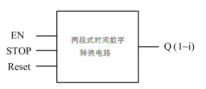
[0026] figure 1 It is the overall block diagram, the input signal of the circuit is the gate control signal EN, the stop pulse signal STOP, and the reset signal Reset, and the output signals are: Q1, Q2, ... Qi, where i is the number of output signals. The circuit works when the gate control signal EN is high level, and the circuit stops working when it is low level. The rising edge of stop pulse signal STOP is valid. When the stop pulse signal STOP is valid, the TDC stops counting, and the circuit outputs the counting result.
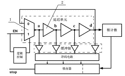
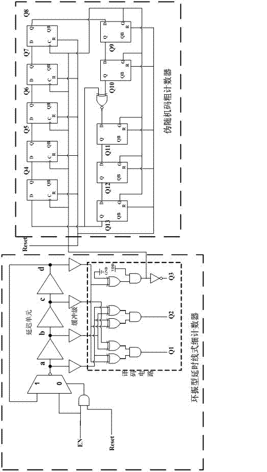
[0027] figure 2 It is the overall structure diagram of the circuit. The circuit is mainly composed of a fine counter part (the first counter part) and a coarse counter part (the second counter part). The fine counter part includes a delay unit, a decoding circuit, a buffer stage, a latch, and a delay unit The circular delay lin...
PUM
 Abstract
Description
Claims
Application Information


