
Triple junction solar cell and preparation method thereof

A solar cell and three-junction technology, applied in the field of solar cells, can solve the problems of insufficient conversion and utilization of solar spectrum energy, increase the difficulty and cost of growth and process, and achieve reduced manufacturing difficulty, small current mismatch, and reduced The effect of small heat loss

Active Publication Date: 2013-07-24
SUZHOU INST OF NANO TECH & NANO BIONICS CHINESE ACEDEMY OF SCI
View PDF3 Cites 0 Cited by
  • Summary
  • Abstract
  • Description
  • Claims
  • Application Information

AI Technical Summary

Problems solved by technology

However, there is still a major problem in this system that the Ge battery covers a wider spectrum, and its short-circuit current can reach twice that of the other two-junction batteries. Due to the constraints of the three-junction batteries connected in series, the energy of the solar spectrum corresponding to the Ge battery is not captured. full conversion
However, GaInP / GaAs / InGaAs (~1.0 eV) triple-junction cells often use an inverted growth method due to a 2.1% lattice mismatch between GaAs and InGaAs cells, and then use techniques such as substrate lift-off to increase the growth rate. and the difficulty and cost of the process

Method used


Image

  • Triple junction solar cell and preparation method thereof
  • Triple junction solar cell and preparation method thereof
  • Triple junction solar cell and preparation method thereof

Examples


Embodiment Construction

[0018] The three-junction solar cell provided by the present invention and its preparation method will be described in detail below with reference to the accompanying drawings.

[0019] First, specific implementations of the three-junction solar cell of the present invention are given in conjunction with the drawings.

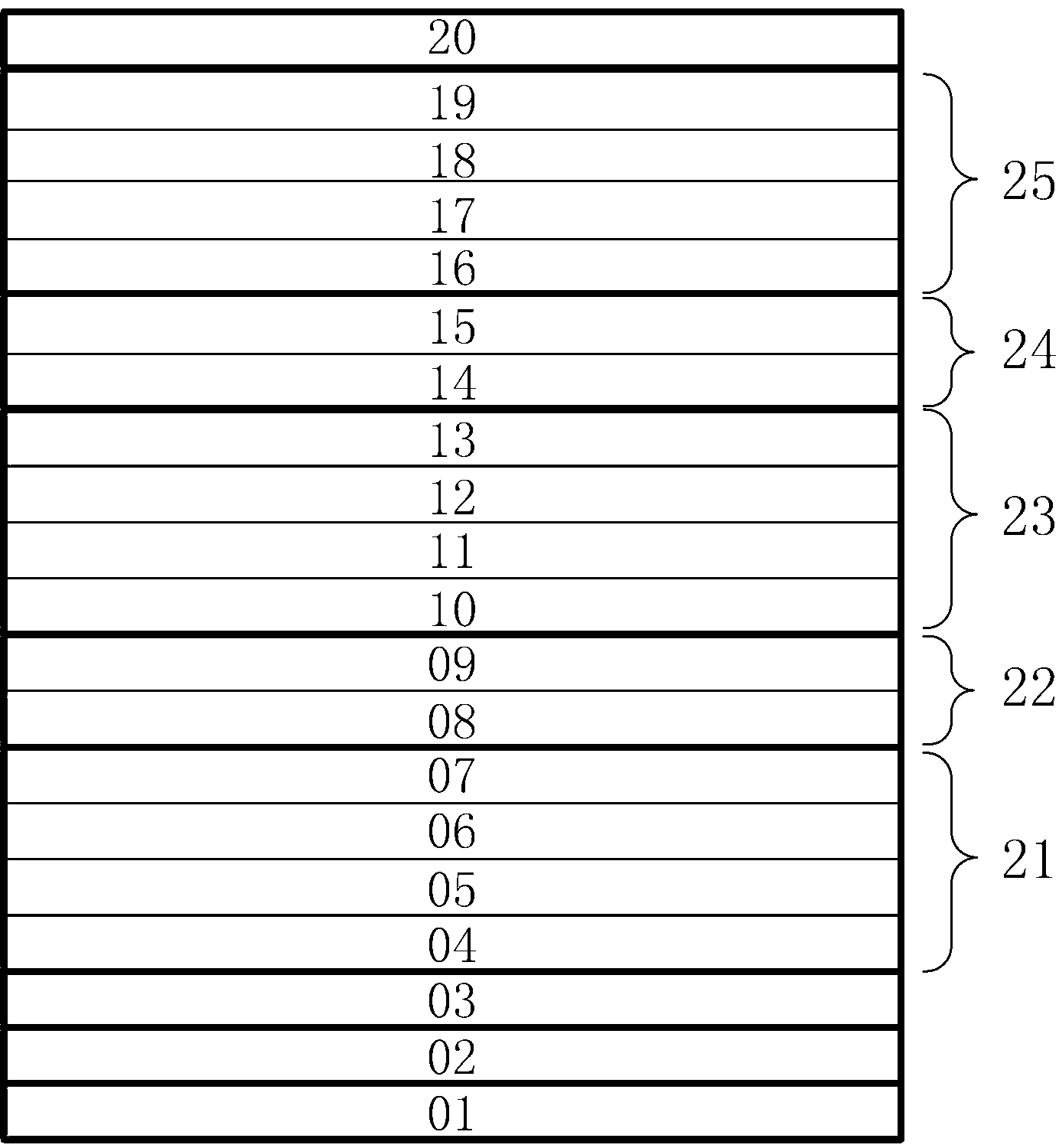
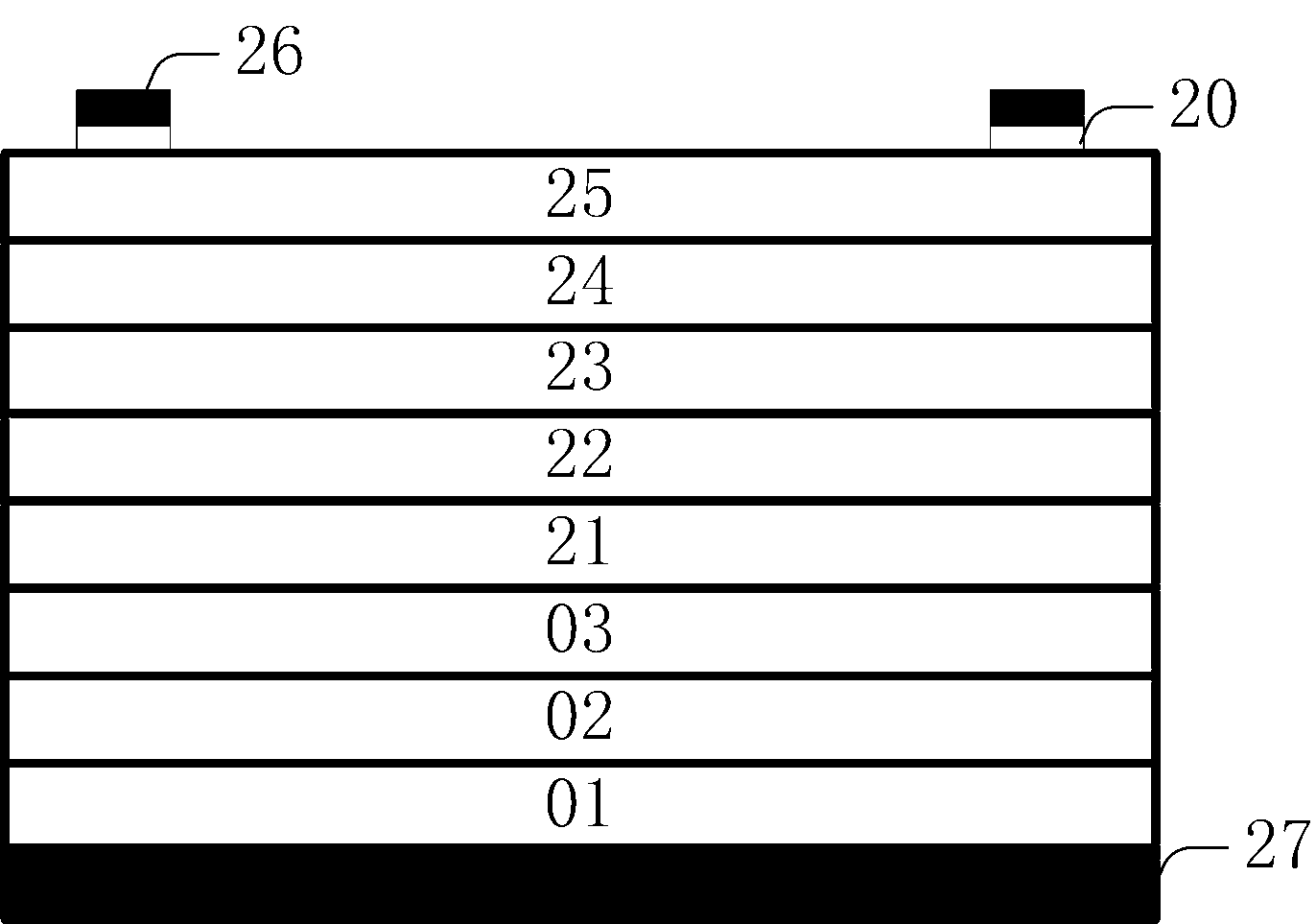
[0020] Reference attachment figure 1 , 2 Shown, where, figure 1 It is a schematic diagram of the structure of the three-junction solar cell provided in this embodiment, figure 2 for figure 1 The structure diagram of the finished product of the three-junction solar cell shown, and then the attached figure 1 , 2 The structure shown is explained in detail.

[0021] This embodiment provides a three-junction solar cell, including: a GaAs substrate 01, an InGaAs bottom cell 21, a first tunnel junction 22, an InGaAsP intermediate cell 23, a second tunnel junction 24, an InAlAs top cell 25, and an ohmic contact layer 20 . The InAlAs top cell 25 and the GaAs substrate 01 are...


PUM


Abstract

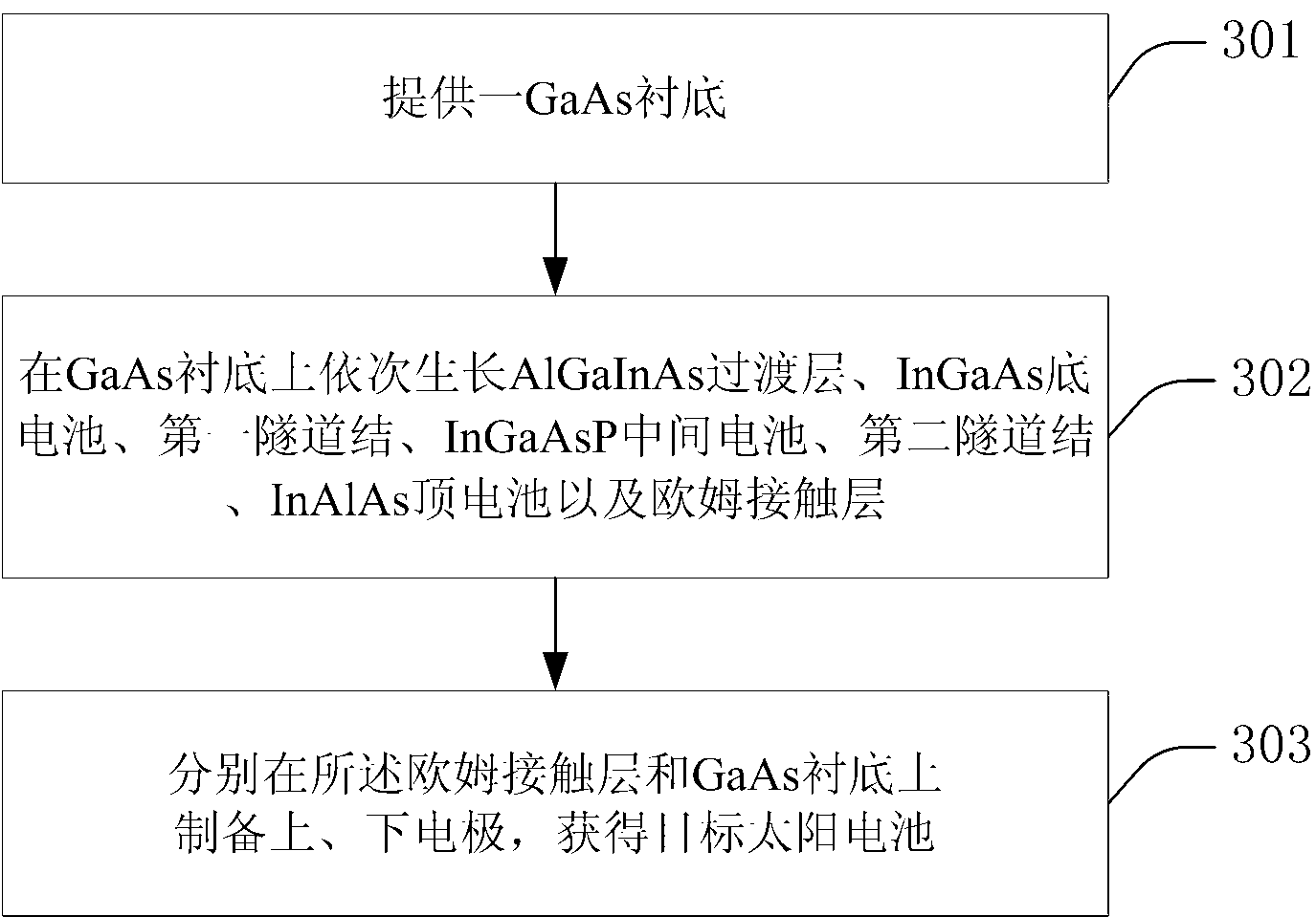
The invention provides a triple junction solar cell and a preparation method of the triple junction solar cell to achieve a reasonable band gap combination of a multi-junction solar cell and to reduce current mismatch without increase in cell manufacturing cost and difficulty. The triple junction solar cell comprises a GaAs substrate, an AlGaInAs transition layer, an InGaAs bottom cell, a first tunnel junction, an InGaAsP middle cell, a second tunnel junction, an InAlAs top cell and an ohmic contact layer, wherein the AlGaInAs transition layer, the InGaAs bottom cell, the first tunnel junction, the InGaAsP middle cell, the second tunnel junction, the InAlAs top cell and the ohmic contact layer are arranged on the GaAs substrate in sequence. Lattice constants among all subsidiary cells are matched, and the band gap combination is 1.93 eV, 1.39 eV, and 0.94 eV. The preparation method of the triple junction solar cell includes the following steps: (1) providing the GaAs substrate; (2) growing the AlGaInAs transition layer, the InGaAs bottom cell, the first tunnel junction, the InGaAsP middle cell, the second tunnel junction, the InAlAs top cell and the ohmic contact layer on the GaAs substrate in sequence; and (3) preparing an upper electrode and a lower electrode on the ohmic contact layer and the GaAs substrate respectively, and obtaining the target solar cell.

Description

Technical field [0001] The present invention relates to the field of solar cells, in particular to a lattice-matched InAlAs / InGaAsP / InGaAs triple-junction solar cell based on a GaAs substrate using a lattice abnormal change buffer layer and a preparation method thereof. Full use of the spectrum, with a theoretical conversion efficiency higher than 51% under concentrating light. Background technique [0002] In the field of III-V solar cells, multi-junction systems are usually used to achieve segmented absorption and utilization of the solar spectrum to obtain higher conversion efficiency. At present, the most researched and more mature systems are GaInP / GaAs / Ge and GaInP / GaAs / InGaAs (~1.0 eV) triple junction batteries. The former currently achieves a maximum conversion efficiency of 32-33% under one sun. However, the main problem of this system is that the Ge battery covers a wide spectrum, and its short-circuit current can reach up to twice that of the other two-junction batte...

Claims


Application Information

Patent Timeline
IPC IPC(8): H01L31/0352H01L31/0687H01L31/18
CPCY02E10/544Y02P70/50
Inventor 于淑珍董建荣李奎龙孙玉润曾徐路赵勇明赵春雨杨辉
Owner SUZHOU INST OF NANO TECH & NANO BIONICS CHINESE ACEDEMY OF SCI
Learn More