GaInP/GaAs/InGaAsP/InGaAs four-junction cascade solar battery and preparation method thereof
A solar cell, alxin1-xas technology, applied in circuits, photovoltaic power generation, electrical components, etc., can solve the problems of increasing battery manufacturing cost and increasing the difficulty of battery manufacturing, and achieve the goal of reducing manufacturing difficulty, improving battery efficiency, and improving mechanical strength Effect
- Summary
- Abstract
- Description
- Claims
- Application Information
AI Technical Summary
Problems solved by technology
Method used
Image
Examples
Embodiment approach
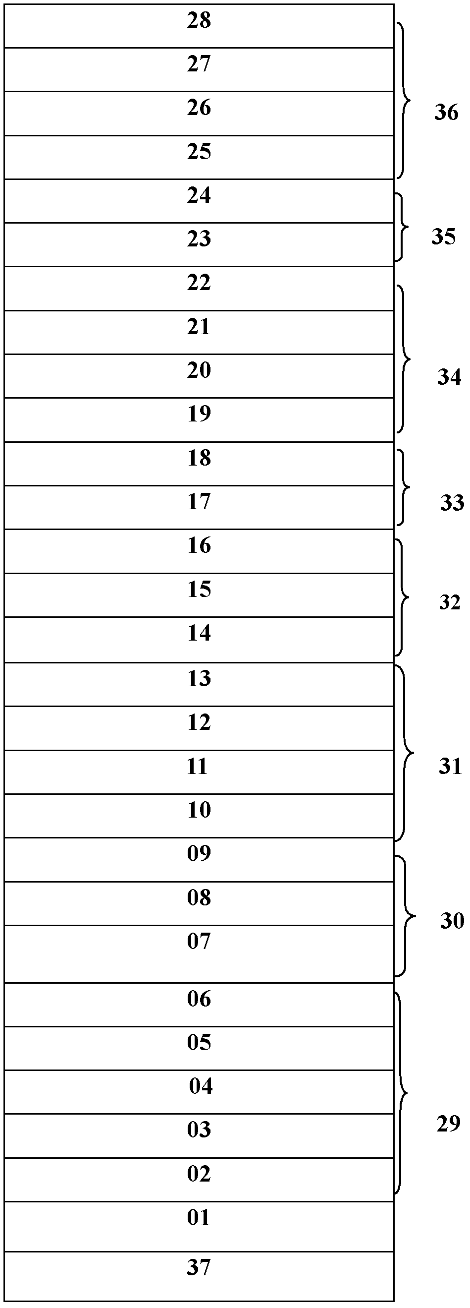
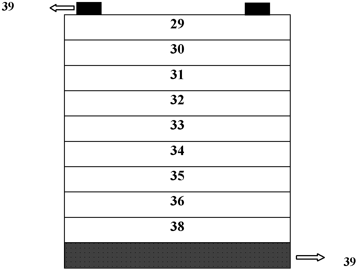
[0072] As a preferred embodiment: the GaInP / GaAs / InGaAsP / InGaAs four-junction cascaded solar cell grown by the lattice transformation method adopts a GaAs or Ge substrate. Specifically, the AlGaAs or (Al)GaInP sacrificial layer and the N-type GaAs contact layer are first grown on the GaAs or Ge substrate, and then the GaInP cell and the GaAs cell are grown in reverse order, and then the Al x In 1-x As gradient transition layer, the composition of Al changes from 1.00 to 0.48, so that it transitions from GaAs lattice constant to InP lattice constant, and finally grows InGaAsP battery and InGaAs battery, and each sub-cell is connected in series through a tunnel junction.
[0073] The growth preparation method of the GaInP / GaAs / InGaAsP / InGaAs four-junction cascaded solar cell includes the following specific steps:
[0074] (1) Growth of GaInP / GaAs / InGaAsP / InGaAs four-junction cascaded solar cells
[0075] (1) growing an AlGaAs or (Al)GaInP sacrificial layer and an N-type doped ...
Embodiment 1
[0093] Embodiment 1: see figure 1 The preparation method of the GaInP / GaAs / InGaAsP / InGaAs four-junction cascaded solar cell grown based on the lattice anomaly growth method comprises the following steps:
[0094](1) GaInP / GaAs / InGaAsP / InGaAs four-junction cascaded solar cells are grown by MOCVD method, and its structure is as follows figure 1 Shown:
[0095] (1) On the GaAs substrate 37, grow 0.3 micron AlGaAs or (Al)GaInP sacrificial layer 01, N-type highly doped 0.5 micron GaAs 02 , forming a contact layer for ohmic contact.
[0096] (2) in GaAs 02 The upper growth N-type doping concentration is about 1′10 17 cm -3 0.02 µm Al(Ga)InP 03 As a GaInP cell 29 The window layer, and then grow the N-type doping concentration of about 1′10 18 cm -3 0.07 µm GaInP 04 As a GaInP cell 29 In the emitter region, the re-growth P-type doping concentration is about 1′10 17 cm -3 0.7 µm GaInP 05 As a GaInP cell 29 the base area;
[0097] (3) Growth P-type doping conc...
PUM
 Abstract
Description
Claims
Application Information

