Light emitting diode device and method of producing the same

A technology of light-emitting diodes and manufacturing methods, applied to electrical components, circuits, semiconductor devices, etc., can solve problems such as high pressure, fragility, deformation and strain of packaging materials, and achieve high pressure, long heating time, and extrusion force uniform effect

Inactive Publication Date: 2013-07-31
NITTO DENKO CORP
View PDF1 Cites 4 Cited by
  • Summary
  • Abstract
  • Description
  • Claims
  • Application Information

AI Technical Summary

Problems solved by technology

[0007] However, in the method described in Japanese Patent Application Laid-Open No. 2011-228525, since the sealing material is sandwiched between press plates and pressurized and heated, there is a problem that the pressure is high and the heating time is long: it is easy to apply a load to the device. , or the packaging material (sheet) is prone to deformation, strain, or breakage

Method used


Image

  • Light emitting diode device and method of producing the same
  • Light emitting diode device and method of producing the same
  • Light emitting diode device and method of producing the same

Examples


preparation example 1

[0227] Preparation of Condensation·Addition Reaction Curable Silicone Resin Composition

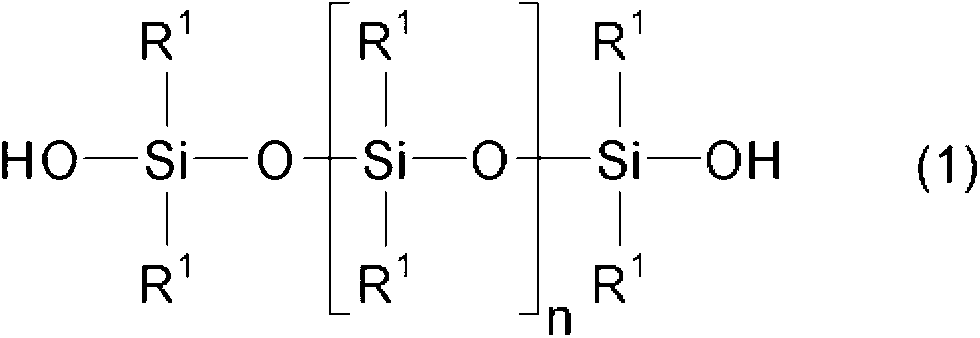
[0228] With respect to the polydimethylsiloxane with both ends of the silanol group (polysiloxane with both ends of the silanol group, in the general formula (1), R 1 All are methyl groups, the average of n is 155, the number average molecular weight is 11500, the silanol group equivalent is 0.174mmol / g) 2031g (0.177mol), and vinyltrimethoxysilane (vinyl silicon compound) is compounded with 15.71g (0.106mol) , and (3-glycidoxypropyl)trimethoxysilane (epoxy group-containing silicon compound) 2.80 g (0.0118 mol) were stirred and mixed.

[0229] Among them, the SiOH group of polydimethylsiloxane at both ends of the silanol group and the SiOCH group of vinyltrimethoxysilane and (3-glycidoxypropyl) trimethoxysilane 3 Molar ratio of groups (moles of SiOH groups / SiOCH 3 total moles of bases) is 1 / 1.

[0230] After stirring and mixing, 0.97 mL (0.766 g, catalyst content: 0.88 mmol) of a meth...

Embodiment 1

[0235] Preparation of resin composition

[0236] 100 parts by mass of the heat-curable silicone resin composition of Preparation Example 1 and 26 parts by mass of YAG:Ce (spherical shape, average particle diameter of 10 μm) were mixed to prepare a liquid encapsulating resin composition at room temperature.

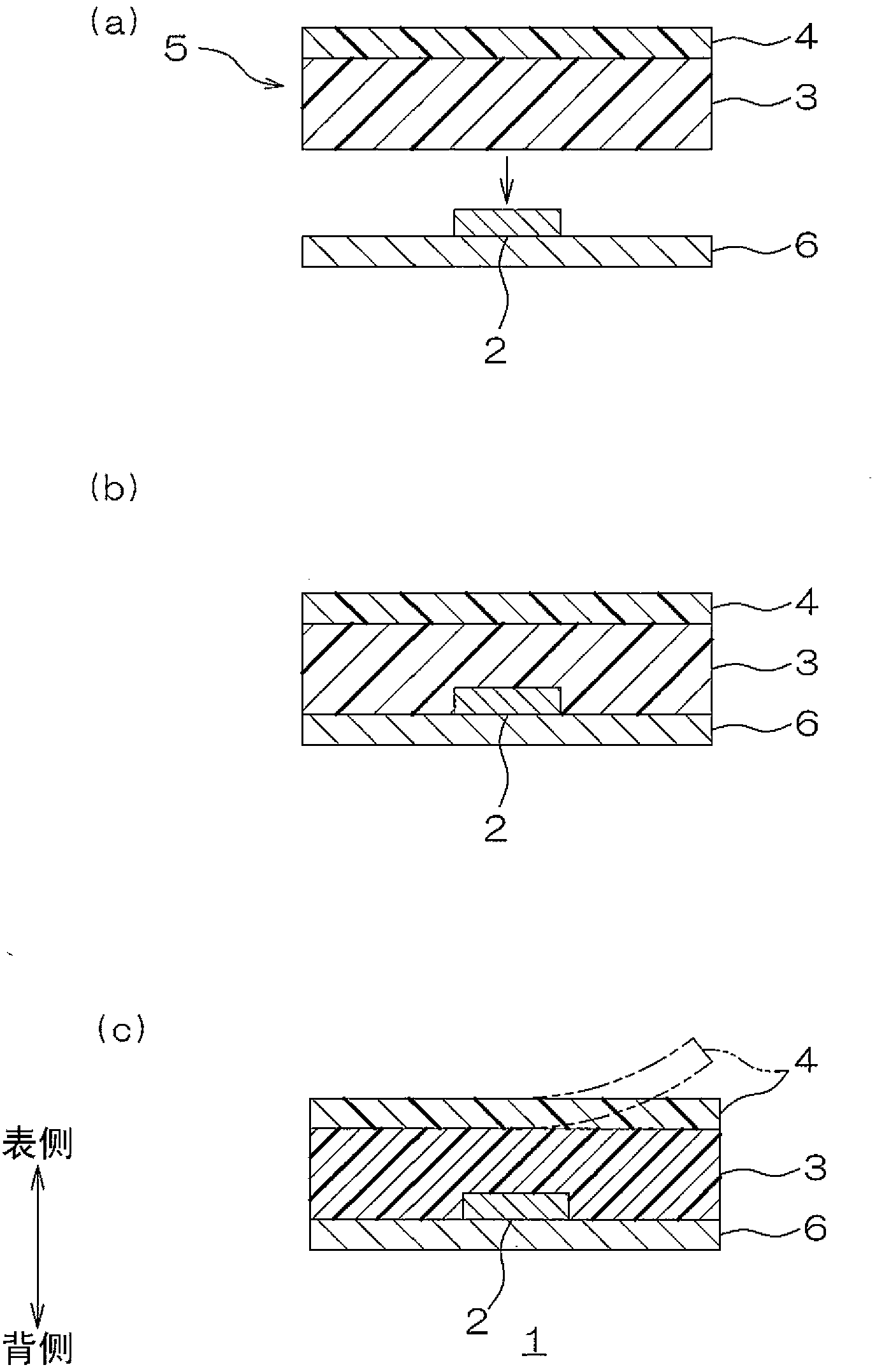
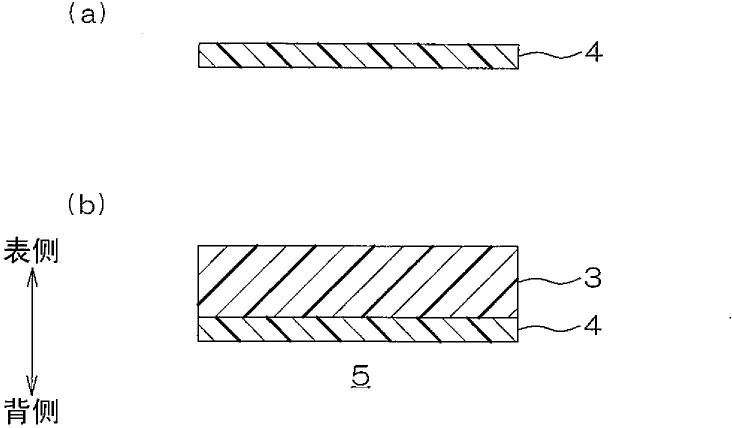
[0237] The encapsulation resin composition prepared is coated on the substrate formed by PET film by doctor blade coating method (referring to figure 2 The entire surface of (a)) was then heated at 135°C for 20 minutes to produce a sealing sheet having a base material and a B-stage sealing resin layer with a thickness of 600 μm laminated on the surface (see figure 2 (b)).

[0238] Thereafter, the package sheet was cut into a 5cm square, and relative to the substrate on which 25 blue light-emitting diode elements (size 0.35mm×0.35mm) were mounted in a 5cm square area, the package sheet was positioned so that they were arranged oppositely (see figure 1 (a)).

[0239]...

Embodiment 2

[0244] Instead of the pressing device in the embedding process, a vacuum pressing device was used to press under a normal temperature and reduced pressure atmosphere, and the same process as in Example 1 was carried out to embed the blue light-emitting diode element in the encapsulating resin layer, and then the The encapsulating resin layer is completely cured, and thereafter, the light emitting diode device is manufactured.

[0245] Among them, the decompression condition of the vacuum pressing device is 1hPa (0.0001MPa).


PUM

PropertyMeasurementUnit
viscosityaaaaaaaaaa
viscosityaaaaaaaaaa
lengthaaaaaaaaaa

Abstract

A method of producing a light emitting diode device (1) includes preparing an encapsulating resin layer; embedding a light emitting diode element in the encapsulating resin layer; and heating while pressing with gas the encapsulating resin layer having the light emitting diode element being embedded therein.

Description

technical field [0001] The present invention relates to a light emitting diode device and a manufacturing method thereof. Specifically, it relates to a light emitting diode device in which a light emitting diode element is encapsulated by a sealing resin layer and a manufacturing method thereof. Background technique [0002] It is known that a light emitting diode device is obtained by encapsulating a light emitting diode element (LED) with an encapsulating resin layer. [0003] For example, the following methods are proposed (For example, refer to Unexamined-Japanese-Patent No. 2011-228525.). [0004] That is, a method has been proposed in which an encapsulating material is formed so as to cover an optical semiconductor element on a substrate mounted with an optical semiconductor element, thereafter, they are sandwiched by pressing plates under reduced pressure in a vacuum pressing device, and The encapsulating material is cured by heating while vacuum pressing, and the op...

Claims


Application Information

Patent Timeline
Patent Type & Authority Applications(China)
IPC IPC(8): H01L33/52H01L33/00
CPCH01L2933/005H01L33/52B29C43/10H01L33/56B29C43/18H01L33/48
Inventor 片山博之大薮恭也佐藤慧
Owner NITTO DENKO CORP
Why Eureka
Try Eureka