Chip bonding structure and bonding method

A chip bonding and chip technology, which is used in semiconductor/solid-state device parts, semiconductor devices, electrical components, etc., and can solve problems such as reducing the reliability of die bonding, overflowing eutectic materials, and poor electrical connection between the chip and the heat dissipation substrate.

Inactive Publication Date: 2013-08-14
LEXTAR ELECTRONICS CORP
View PDF5 Cites 3 Cited by
  • Summary
  • Abstract
  • Description
  • Claims
  • Application Information

AI Technical Summary

Problems solved by technology

[0003] Eutectic soldering technology can coat flux (flux) on the heat dissipation substrate to help the metal components on the heat dissipation substrate and the metal components of the eutectic material to diffuse each other. After the chip is bonded to the heat dissipation substrate, a reflow step is required. The flux is liquid and fluid during soldering, which makes the position of the chip easy to shift, resulting in poor electrical connection between the chip and the heat dissipation substrate, resulting in a decrease in the packaging yield of the chip
[0004] Another eutectic soldering technique is to use the down pressure to help the metal components on the heat dissipation substrate and the metal components of the eutectic material to diffuse with each other without coating flux. Poor stability reduces the reliability of die bonding

Method used


Image

  • Chip bonding structure and bonding method
  • Chip bonding structure and bonding method
  • Chip bonding structure and bonding method

Examples


Embodiment Construction

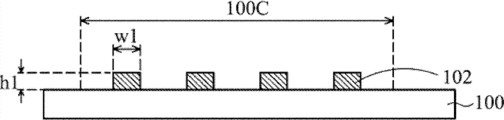
[0023] refer to Figure 1A to Figure 1C , which shows a schematic cross-sectional view of each stage of a bonding method of a chip bonding structure according to an embodiment of the present invention. Figure 1A Firstly, a substrate 100 for fixing the chip is provided, such as a printed circuit board, a ceramic substrate, a metal substrate such as copper or aluminum, the substrate 100 has a chip predetermined area 100C, and a plurality of bumps (bump) 102 are arranged on the chip predetermined area 100C. on the surface of the substrate 100. The material of the bump 102 can be gold, silver, copper, the aforementioned alloys or other metal materials. In one embodiment, a wire bonder can be used to form a plurality of metal balls in the chip predetermined area 100C of the substrate 100. Then carry out the leveling step to flatten the surface of the metal ball to form a Figure 1A A plurality of bumps 102 that are flush with the surface are shown.

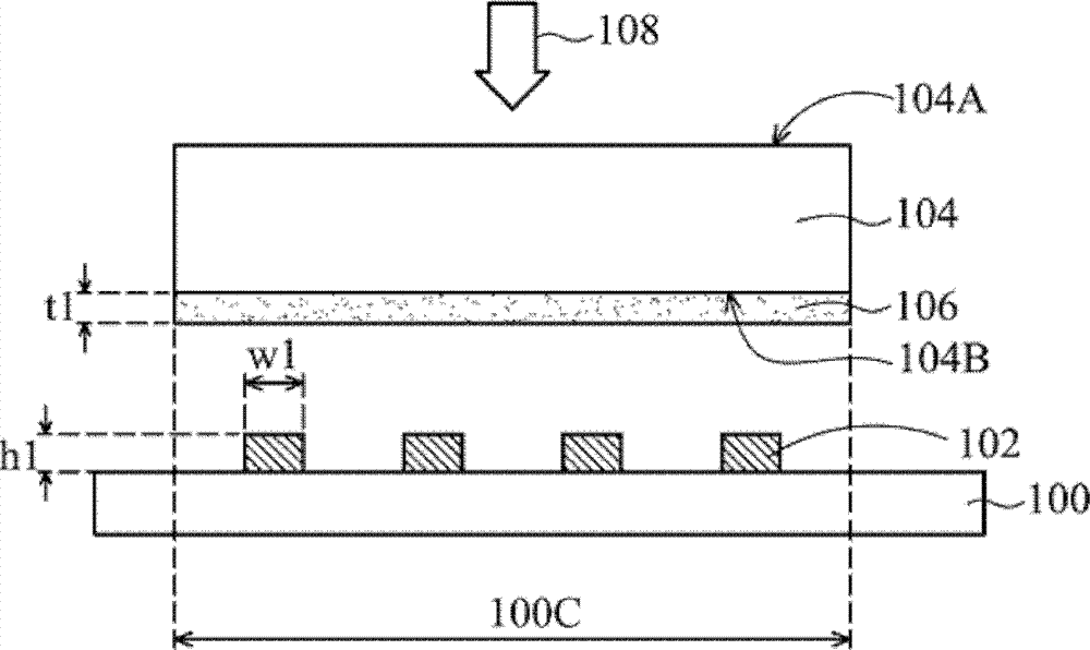
[0024] Figure 1B Provide a...


PUM


Abstract

The present invention discloses a chip bonding structure and a bonding method, and the chip bonding structure comprises a baseplate that contains a chip predetermined area, and the surface of the chip predetermined area is provided with a plurality of protrusions on the baseplate; the chip has a luminous front side and a back side corresponding to the luminous front side; and the back side is provided with an eutectic bonding material layer with a plurality of depressed structure, wherein each depressed structure bonds with each protrusion, and that makes the chip fixed on the chip predetermined area of the baseplate.

Description

technical field [0001] The invention relates to a chip bonding technology, in particular to a chip bonding structure and a chip bonding method for avoiding chip offset. Background technique [0002] Generally speaking, chip packaging needs to fix the chip on the heat dissipation substrate. The traditional die bonding technology can be divided into silver colloidal die bonding, eutectic soldering and flip chip soldering. Among them, the eutectic soldering technology is Form the eutectic material on the back of the chip, heat the heat dissipation substrate and the eutectic material to the eutectic temperature of the eutectic material, and allow the metal component of the eutectic material to diffuse with the metal component on the heat dissipation substrate, thereby changing the composition of the eutectic material By increasing its melting point, the eutectic material is solidified, and the chip is fixed on the heat dissipation substrate. [0003] Eutectic soldering technolo...

Claims


Application Information

Patent Timeline
Patent Type & Authority Applications(China)
IPC IPC(8): H01L23/488H01L21/60
CPCH01L2224/83193H01L2224/83191H01L24/83H01L2224/16225H01L2224/73204H01L2224/32225H01L2924/01322H01L2224/83385H01L2924/12041H01L2924/15787H01L2924/00
Inventor 邱冠谕
Owner LEXTAR ELECTRONICS CORP
Why Eureka
Try Eureka