Surface acoustic wave type touch control panel and method for manufacturing the same
A surface acoustic wave, touch panel technology, applied in the touch panel and its manufacturing field, can solve the problems of applicability limitation, fatigue, low sensitivity, etc.
- Summary
- Abstract
- Description
- Claims
- Application Information
AI Technical Summary
Problems solved by technology
Method used
Image
Examples
Embodiment 1
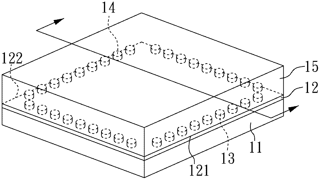
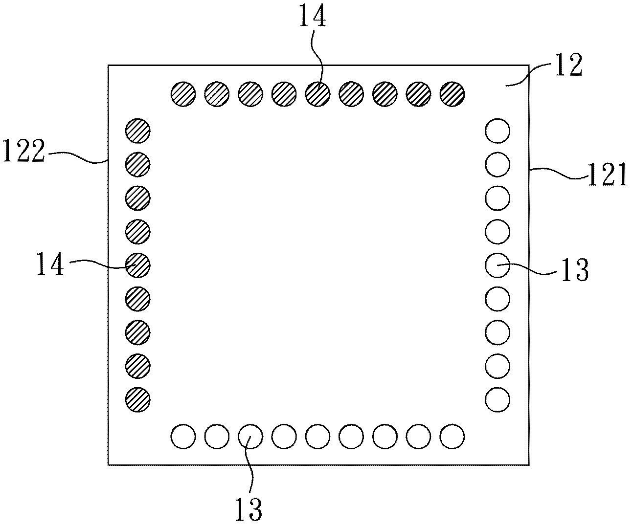
[0036] refer to Figure 1A and Figure 1B and Figure 2A ,in, Figure 1A is a structural schematic diagram of a surface acoustic wave touch panel of the present invention, Figure 1B yes Figure 1A sectional schematic diagram of Figure 2A is a schematic diagram of the electrode setup on the surface of the piezoelectric material layer.
[0037] Such as Figure 1A As shown, a substrate 11 is firstly provided, wherein the substrate 11 can be a transparent substrate, such as a glass substrate, a quartz substrate or a sapphire substrate. In this embodiment, a glass substrate is used as the substrate 11 .
[0038] Then, a piezoelectric material layer 12 is formed on the surface of the substrate 11 , wherein the piezoelectric material layer 12 has a first side edge 121 and a second side edge 122 opposite to the first side edge 121 . In this embodiment, the piezoelectric material layer 12 is an aluminum nitride layer, but the material and structure of the piezoelectric material l...
Embodiment 2
[0043] The method of manufacturing the surface acoustic wave touch panel in this embodiment is substantially the same as that of the first embodiment above, the difference lies in the arrangement of the voltage supply electrode and the voltage receiving electrode in this embodiment refer to Figure 2B , Figure 2B It is a schematic diagram of the voltage supply electrode 13 and the voltage reception electrode 14 on the surface of the piezoelectric material layer 12 .
[0044] Such as Figure 2B As shown, the piezoelectric material layer 12 has a first side edge 121, a second side edge 122 opposite to the first side edge, and a first side edge 121 adjacent to the second side edge 122. There are three side edges 123 , and the voltage supply electrode 13 and the voltage receiving electrode 14 are arranged at intervals along the direction of the first side edge 121 and the direction of the third side edge 123 .
Embodiment 3
[0046] The method of manufacturing the surface acoustic wave touch panel in this embodiment is substantially the same as that of the first embodiment above, the difference lies in the arrangement of the voltage supply electrode and the voltage receiving electrode in this embodiment refer to Figure 2C , Figure 2C It is a schematic diagram of the voltage supply electrode 13 and the voltage reception electrode 14 on the surface of the piezoelectric material layer 12 .
[0047] Such as Figure 2C As shown, the piezoelectric material layer 12 has a first side edge 121, a second side edge 122 opposite to the first side edge, and a first side edge 121 adjacent to the second side edge 122. There are three side edges 123 , and the voltage supply electrodes 13 and the voltage receiving electrodes 14 are respectively arranged in a row along the direction of the first side edge 121 and arranged at intervals along the direction of the third side edge 123 .
[0048] In summary, the pres...
PUM
 Abstract
Description
Claims
Application Information


