Manufacturing method of through hole interconnection structure and product of through hole interconnection structure

An interconnection structure and manufacturing method technology, applied in the fields of semiconductor/solid-state device manufacturing, electrical components, circuits, etc., can solve the problems of long process flow and low efficiency, and achieve the effect of simplifying process steps, easy to control, and high filling quality

Inactive Publication Date: 2013-08-21
HUAZHONG UNIV OF SCI & TECH
View PDF3 Cites 12 Cited by
  • Summary
  • Abstract
  • Description
  • Claims
  • Application Information

AI Technical Summary

Problems solved by technology

However, the production of the seed layer in this method generally requires additional process steps, such as making auxiliary wafers and temporary bonding of the auxiliary wafers; or it is necessary to pre-fill the seed layer and electroplating on the back of the wafer to be plated; therefore, there is a long process flow and high efficiency. Defects such as inferiority

Method used


Image

  • Manufacturing method of through hole interconnection structure and product of through hole interconnection structure
  • Manufacturing method of through hole interconnection structure and product of through hole interconnection structure
  • Manufacturing method of through hole interconnection structure and product of through hole interconnection structure

Examples


Embodiment Construction

[0034] In order to make the object, technical solution and advantages of the present invention clearer, the present invention will be further described in detail below in conjunction with the accompanying drawings and embodiments. It should be understood that the specific embodiments described here are only used to explain the present invention, not to limit the present invention.

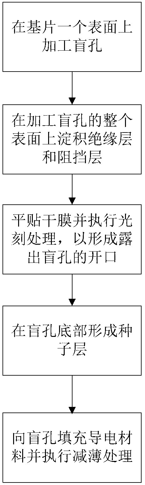
[0035] figure 1 It is a schematic diagram of a process flow for making a through-silicon via interconnection structure according to the present invention. Such as figure 1 Shown in, according to the fabrication method of the via interconnection structure of the present invention mainly comprises the following steps:

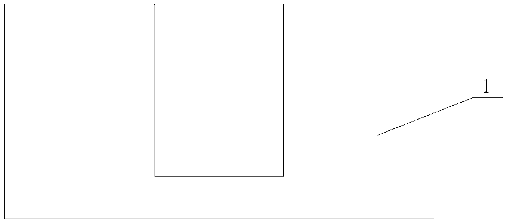
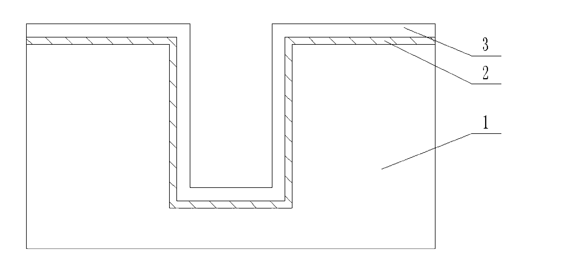
[0036] First, refer to Figure 2a As shown in , a blind hole is processed on one surface of the substrate 1 (shown as the upper surface in the figure), and the depth of the blind hole is not less than its diameter. The substrate can be made of semiconductor materials, such as elem...


PUM


Abstract

The invention discloses a manufacturing method of a through hole interconnection structure. The manufacturing method of the through hole interconnection structure comprises the following steps: (a) a blind hole is machined in one surface of a substrate; (b) an insulating layer and a barrier layer are deposited on the whole surface in sequence, where the blind hole is machined, of the substrate; (c) a light-sensitive dry film is paved on and attached to the surface, containing the barrier layer, of the substrate, and exposure imaging treatment is carried out on the surface, so that an opening exposed out of the blind hole is formed; (d) the dry film is used as a covering film, a seed layer is formed on the barrier layer on the bottom of the blind hole, and the seed layer is prevented from covering the barrier layer deposited on the lateral wall of the blind hole; (e) growth from bottom to top is achieved with the seed layer on the bottom of a through hole as guiding media, and the thickness of another surface of the substrate is reduced until the blind hole is machined to be the through hole. The invention further discloses a product of the through hole interconnection structure. According to the manufacturing method of the through hole interconnection structure and the product of the through hole interconnection structure, through hole electroplating which is convenient to control, low in cost, and high in efficiency can be achieved, and the product of the through hole interconnection structure and with better filling effect can be obtained.

Description

technical field [0001] The invention belongs to the technical field of semiconductor packaging, and more specifically relates to a method for manufacturing a through-hole interconnection structure and a product thereof. Background technique [0002] At the beginning of the development of the integrated circuit industry, people have continuously reduced the key dimensions and continuously improved the integration of chips to obtain high-performance semiconductor chips. However, when the critical dimension continues to shrink, it brings many problems such as a sharp increase in the implementation cost of the lithography process and limitations in the physical properties of the material. In order to better realize three-dimensional stack packaging, through-silicon via (TSV, Through Silicon Via) technology emerges as needed. The so-called through-silicon via technology is a new solution to realize the interconnection between chips by making vertical conduction between chips and...

Claims


Application Information

Patent Timeline
Patent Type & Authority Applications(China)
IPC IPC(8): H01L21/768
Inventor 廖广兰史铁林薛栋民独莉张昆宿磊陆向宁
Owner HUAZHONG UNIV OF SCI & TECH
Why Eureka
Try Eureka