Manufacturing method of COA array substrate, array substrate and display device

An array substrate and substrate technology, applied in semiconductor/solid-state device manufacturing, optics, instruments, etc., can solve the problems of low production efficiency, high cost, and complex array substrate preparation methods, and achieve low cost, good fluidity, and cost savings. Effect

Inactive Publication Date: 2013-08-21
BOE TECH GRP CO LTD
View PDF4 Cites 13 Cited by
  • Summary
  • Abstract
  • Description
  • Claims
  • Application Information

AI Technical Summary

Problems solved by technology

[0004] The technical problems to be solved by the present invention include, aiming at the problems of complex preparation methods, low production efficiency and high cost of the existing array substrates, providing a method for preparing array substrates that can reduce manufacturing processes, reduce costs, and improve production efficiency , array substrate and display device

Method used


Image

  • Manufacturing method of COA array substrate, array substrate and display device
  • Manufacturing method of COA array substrate, array substrate and display device
  • Manufacturing method of COA array substrate, array substrate and display device

Examples


Embodiment 1

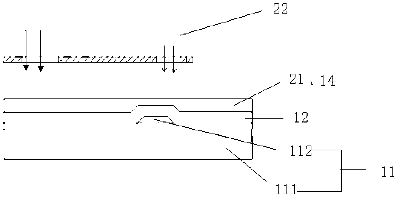
[0025] combine image 3 , Figure 4 , Figure 5 , this embodiment provides a method for preparing a COA array substrate, including:

[0026] Step 1, first fabricate thin film transistors 112, metal wires and other components on the substrate 111, complete the fabrication of the TFT substrate 11, and make a protective layer 12 on the TFT substrate 11 to protect the backplane.

[0027] Step 2, coat the photoresist layer 21 on the protective layer 12, and use the mask plate 22 to expose the photoresist layer 21 through the patterning process. The exposed area is the color pixel area. After the exposure, the color pixel area is developed and post-baked A color filter receiving hole 32 is fabricated, and the photoresist layer 21 serves as a planarization layer 14 at the same time.

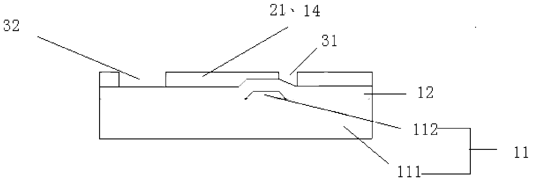
[0028] Step 3, adding dyes to the color filter receiving holes 32 to form the color filter layer 13 . Wherein, since the step difference of the photoresist layer 21 is very small, the photoresist la...

Embodiment 2

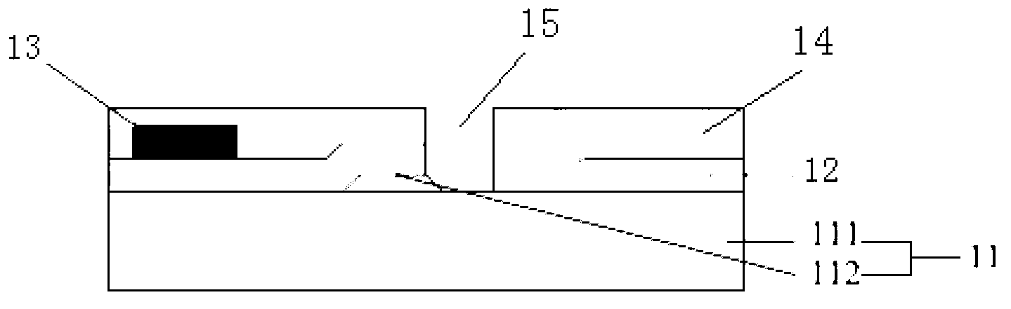
[0041] This embodiment provides an array substrate, including a photoresist layer 21 on the protective layer 12, the photoresist layer 21 also serves as a planarization layer 14, and a color filter receiving hole 32 is formed therein, the color filter receiving hole 32 is formed with a color filter layer 13 . The photoresist serves as the planarization layer 14 at the same time, which can save costs during fabrication.

[0042] Preferably, the array substrate is an OLED substrate, and a via hole 15 is provided on the COA array substrate, and the anode is connected to the drain of the thin film transistor 112 on the OLED substrate through the via hole 15 . Of course, the OLED can also be arranged on the TFT substrate 11 , and the anode of the OLED is directly connected to the drain of the thin film transistor 112 , so the array substrate does not need to be provided with the via hole 15 .

[0043]Preferably, the array substrate is a TFT-LCD array substrate, the COA array subst...

Embodiment 3

[0046] This embodiment provides a display device, which includes the above-mentioned array substrate, and of course also includes structures such as an outer frame of a conventional display device.

[0047] Since the display device includes the above-mentioned array substrate, its manufacturing process is simple and the cost is low.


PUM


Abstract

The invention provides a manufacturing method of a COA array substrate, the array substrate and a display device, and belongs to the technical field of liquid crystal display. The manufacturing method of the COA array substrate, the array substrate and the display device can resolve the problems that an existing array substrate is complex in manufacturing method and high in cost. The manufacturing method of the COA array substrate includes the following steps: a photo-etching glue layer is coated on a protective layer on a TFT base, the photo-etching glue layer can be used as a planarization layer at the same time, and the TFT base comprises a base body and a TFT; through a photolithography technique, a colorful-film containing hole is formed in the photo-etching glue layer; a colorful filter layer is manufactured in the colorful-film containing hole. The array substrate comprises the photo-etching glue layer which is located on the protective layer, the photo-etching glue layer can be used as the planarization layer at the same time, the colorful-film containing hole is formed in the photo-etching glue layer, and the colorful filter layer is formed in the colorful-film containing hole. The display device comprises the array substrate.

Description

technical field [0001] The invention belongs to the technical field of liquid crystal display, and in particular relates to a preparation method of a COA array substrate, an array substrate and a display device. Background technique [0002] The COA array substrate means that the color filter layer 13 is fabricated on the TFT substrate 11 (the TFT substrate includes a substrate 111 and a thin film transistor (TFT) 112). Through this design, the width of the black matrix can be reduced and the aperture ratio of the display area can be increased. , the structure of the existing COA array substrate is as follows figure 1 as shown, figure 2 is a schematic diagram of the exposure process for forming the via hole 15 . [0003] At present, the method of making the color filter layer on the TFT substrate is mainly through the patterning process or the inkjet printing method. The current inkjet printing method needs to make a separate retaining wall structure. After the color filt...

Claims


Application Information

Patent Timeline
Patent Type & Authority Applications(China)
IPC IPC(8): H01L21/77H01L27/12H01L27/32G02F1/136
CPCG02F1/1362H01L27/1259H01L2924/0002G02F1/136222H01L2924/00G02F1/1368H01L21/76802H01L21/76877H01L23/535H10K59/123H10K59/38H10K71/00H10K59/1201
Inventor 齐永莲舒适惠官宝
Owner BOE TECH GRP CO LTD
Why Eureka
Try Eureka