Array substrate, display device, and method for manufacturing the array substrate

The technology of an array substrate and manufacturing method, which is applied in the field of display, can solve the problems of low panel aperture ratio and transmittance, and achieve the effects of increasing aperture ratio and transmittance, high resolution, and reducing line width

Active Publication Date: 2015-11-25
BOE TECH GRP CO LTD +1
View PDF6 Cites 0 Cited by
  • Summary
  • Abstract
  • Description
  • Claims
  • Application Information

AI Technical Summary

Problems solved by technology

[0007] The disadvantage of the existing technology is that due to the existence of the common electrode lines on the array substrate, the black matrix on the color filter substrate will cover the common electrode lines, resulting in low aperture ratio and transmittance of the panel.

Method used


Image

  • Array substrate, display device, and method for manufacturing the array substrate
  • Array substrate, display device, and method for manufacturing the array substrate
  • Array substrate, display device, and method for manufacturing the array substrate

Examples


Embodiment Construction

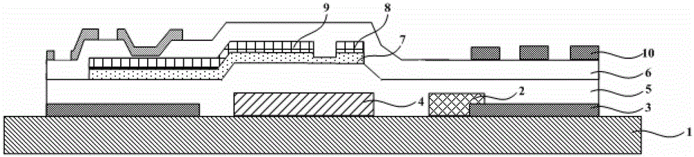
[0044] In order to increase the panel aperture ratio, the present invention provides an array substrate, a display device and a manufacturing method of the array substrate. In this technical solution, since the common electrode lines are located below the scanning lines, the line width of the black matrix on the color filter substrate can be reduced correspondingly, thereby improving the panel aperture ratio and transmittance, and between the scanning lines and the common electrode lines. The electrode lines are separated by an insulating layer, which effectively reduces the storage capacitance, thereby shortening the charging time of the pixel. In order to make the purpose, technical solution and advantages of the present invention clearer, the following specific examples are given to further describe the present invention in detail.

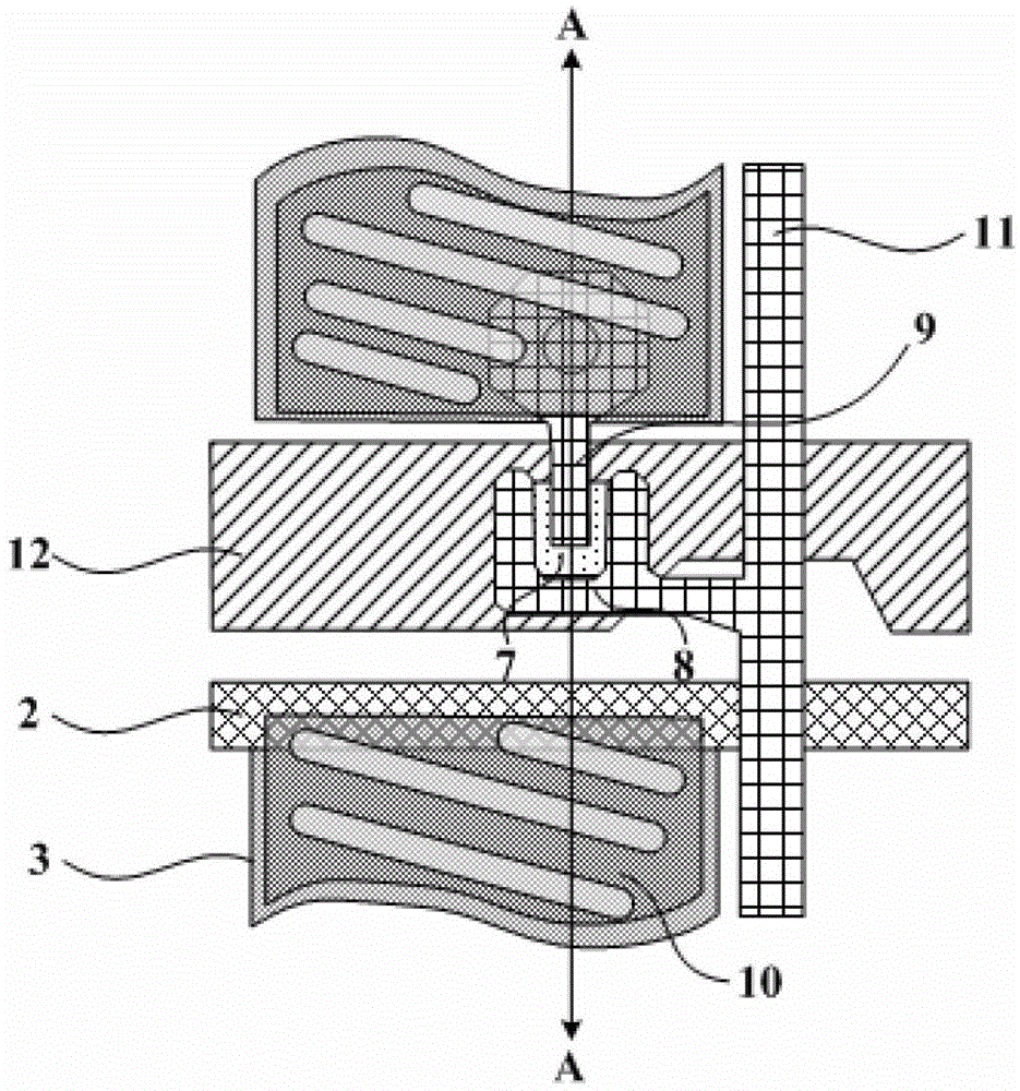
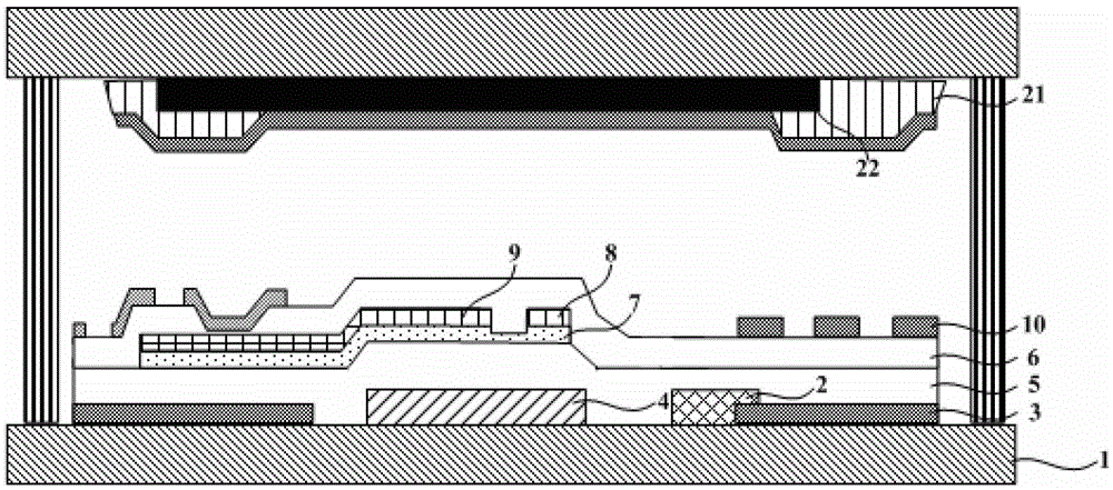
[0045] like Figure 4 As shown, a schematic structural diagram of an embodiment of the array substrate of the present invention, Figure 5 f...


PUM


Abstract

An array substrate, a display apparatus, and a manufacturing method for the array substrate are provided. The array substrate comprises: an underlayer substrate (1); scanning lines (12) and data lines (11) that cross each other and are located on the underlayer substrate (1), the scanning lines (12) and the data lines (11) defining multiple pixel areas; multiple thin film transistors, arranged in an array and respectively located in each pixel area; pixel electrodes (10), located in the pixel areas, and a common electrode (3); an insulation layer (13), located between the common electrode (3) and the scanning lines (12), an projection of the scanning lines (12) on the underlayer substrate (1) at least partially overlapping an projection of a common electrode line (2) on the underlayer substrate (1).

Description

technical field [0001] The present invention relates to the field of display technology, in particular to an array substrate, a display device and a manufacturing method of the array substrate. Background technique [0002] Among flat panel display devices, Thin Film Transistor Liquid Crystal Display (TFT-LCD) has the characteristics of small size, low power consumption, relatively low manufacturing cost and no radiation, and occupies a dominant position in the current flat panel display market. [0003] At present, the display modes of TFT-LCD mainly include TN (TwistedNematic, twisted nematic) mode, VA (VerticalAlignment, vertical orientation) mode, IPS (In-Plane-Switching, plane direction conversion) mode and AD-SDS (ADvancedSuperDimensionSwitch, advanced Ultra-dimensional field conversion technology, referred to as ADS) mode, etc. [0004] Among them, the display based on the ADS mode forms a multi-dimensional electric field through the electric field generated by the e...

Claims


Application Information

Patent Timeline
Patent Type & Authority Patents(China)
IPC IPC(8): G02F1/1362G02F1/1368H01L21/336
CPCG02F1/136286G02F1/133512G02F1/133707G02F2001/13629G02F2201/40H01L27/124G02F1/13629
Inventor 吴洪江
Owner BOE TECH GRP CO LTD
Why Eureka
Try Eureka