Compensation method and compensation circuit for AMOLED threshold voltage

A technology of threshold voltage and compensation method, which is applied in the field of microelectronics to achieve the effect of reducing adverse effects

Active Publication Date: 2013-09-04
SHANGHAI ADVANCED RES INST CHINESE ACADEMY OF SCI
View PDF5 Cites 35 Cited by
  • Summary
  • Abstract
  • Description
  • Claims
  • Application Information

AI Technical Summary

Problems solved by technology

[0004] In view of the above-mentioned shortcomings of the prior art, the purpose of the present invention is to provide a compensation method and compensation circuit for the AMOLED threshold voltage, which is used to solve the problem that the prior art cannot compensate the threshold voltage of the drive tube while reducing the OLED anode point. The impact of the kickback voltage on the drive current caused by the parasitic capacitance between the gate and the drive tube

Method used


Image

  • Compensation method and compensation circuit for AMOLED threshold voltage
  • Compensation method and compensation circuit for AMOLED threshold voltage
  • Compensation method and compensation circuit for AMOLED threshold voltage

Examples


Embodiment 1

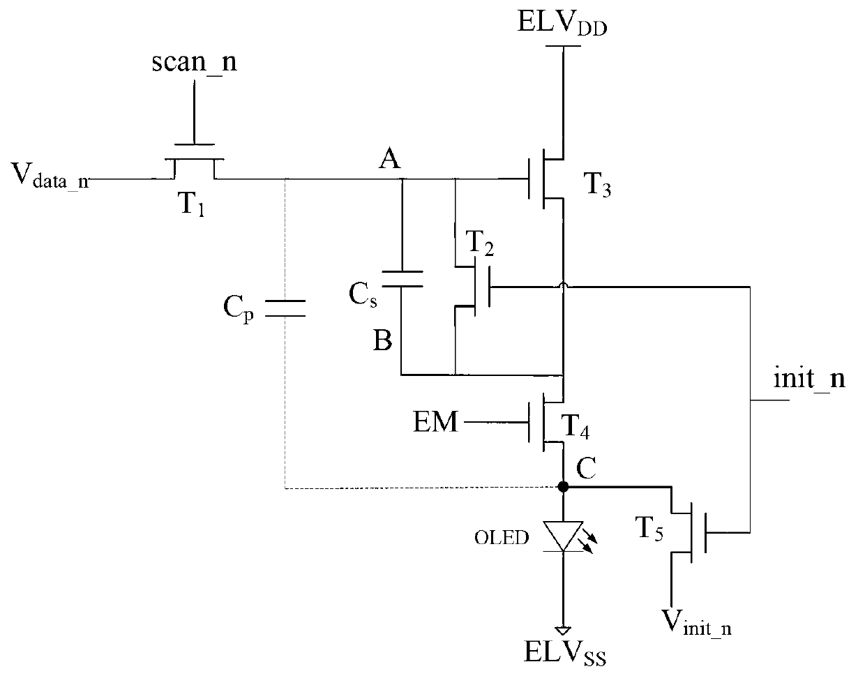
[0027] This embodiment provides a compensation circuit for AMOLED threshold voltage, such as figure 1 As shown, the compensation circuit includes: a scan transistor T1, a reset transistor T2, a drive transistor T3, a light emission control transistor T4, and an initialization transistor T5.

[0028] Among them, the scan transistor T1 controls the image data V data_n Whether to input into the pixel unit; the gate of the scanning transistor T1 is connected to the scanning signal scan_n, and the drain is connected to the image data V data_n .

[0029] The driving transistor T3 drives the OLED to emit light according to the image data; the gate of the driving transistor T3 is connected to the source of the scanning transistor T1.

[0030] The light emission control transistor T4 controls the on-off of the drive transistor T3 and the OLED; the gate of the light emission control transistor T4 is connected to the light emission control signal EM, the drain is connected to the sourc...

Embodiment 2

[0051] This embodiment provides a compensation method for the threshold voltage of an AMOLED, which can be implemented by the compensation circuit described in the first embodiment, but the realized structure is not limited to the circuit structure described in the first embodiment. The compensation method includes the following steps:

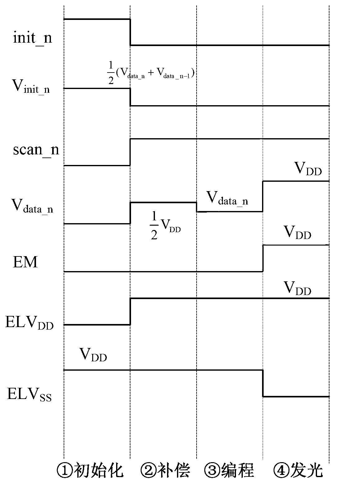
[0052] Initialization steps: set the scanning signal to low level, so that the image data will not be input into the pixel unit; set the light control signal to low level, so that the drive transistor is disconnected from the OLED, so that the OLED will not emit light; set the cathode connection of the OLED High level, make the OLED reverse bias, ensure that the initialization voltage is added to the anode of the OLED; the initialization voltage is the arithmetic mean value or the geometric mean value of the OLED anode point voltage of the previous frame and the OLED anode point voltage of the current frame; set the driving transistor The drai...

Embodiment 3

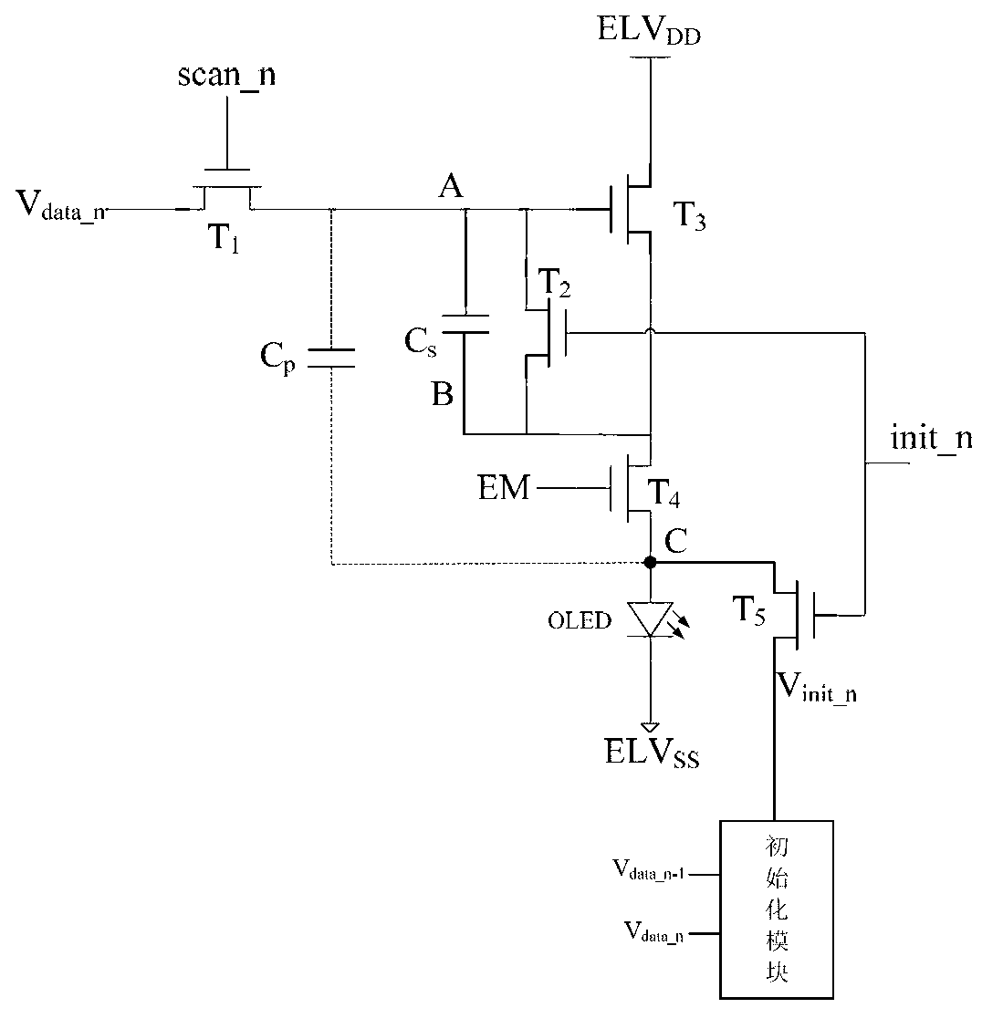
[0061] This embodiment provides a compensation circuit for the AMOLED threshold voltage. The compensation circuit adds an initialization module that provides an initialization voltage on the basis of the circuit structure described in Embodiment 1, and can also realize the compensation circuit for the AMOLED threshold voltage described in Embodiment 2. compensation methods such as image 3 As shown, the initialization module has two input terminals, the input voltages are the OLED anode point voltage of the previous frame and the OLED anode point voltage of the current frame respectively, and the output voltages of the initialization module are the OLED anode point voltage of the previous frame and the current OLED anode point voltage Arithmetic mean or geometric mean of frame OLED anode point voltage.

[0062] The compensation method and compensation circuit for the AMOLED threshold voltage of the present invention not only realize the compensation of the threshold voltage of...


PUM


Abstract

The invention provides a compensation method and a compensation circuit for AMOLED threshold voltage. The compensation circuit comprises a scanning transistor, a driving transistor, a light emitting control transistor, an initialization transistor and a zero clearing transistor, wherein the scanning transistor controls whether image data are input into a pixel unit, the grid electrode of the scanning transistor receives scanning signals, and the drain electrode of the scanning transistor receiving the image data; the driving transistor drives an OLED to emit light according to the image data, and the grid electrode of the driving transistor is connected with the source electrode of the scanning transistor; the light emitting control transistor controls connection and disconnection between the driving transistor and the OLED, the grid electrode of the light emitting control transistor receives light emitting control signals, the drain electrode of the light emitting control transistor is connected with the source electrode of the driving transistor, and the source electrode of the light emitting control transistor is connected with the positive electrode of the OLED; the initialization transistor controls initialization voltage of the positive electrode of the OLED, the drain electrode of the initialization transistor is connected with the initialization voltage, the source electrode of the initialization transistor is connected with the positive electrode of the OLED, and the grid electrode of the initialization transistor receives initialization control signals; the zero clearing transistor carries out zero clearing on electric charges between the grid electrode and the source electrode of the driving transistor, the drain electrode of the zero clearing transistor is connected with the grid electrode of the driving transistor, the source electrode of the zero clearing transistor is connected with the source electrode of the driving transistor, and the grid electrode of the zero clearing transistor receives the initialization control signals. By means of the compensation method and the compensation circuit for the AMOLED threshold voltage, compensation for the threshold voltage of a driving tube is achieved, and bad influences, from back flushing voltage caused by stray capacitance, on driving current are reduced.

Description

technical field [0001] The invention belongs to the technical field of microelectronics, and relates to a compensation circuit and a method, in particular to a compensation method and a compensation circuit for an AMOLED threshold voltage. Background technique [0002] Compared with traditional liquid crystal panels, AMOLED (Active Matrix / Organic Light Emitting Diode, active matrix organic light emitting diode panel) has the characteristics of faster response speed, higher contrast ratio, and wider viewing angle. The driving of AMOLED is the key to OLED display technology. At present, there are some problems in AMOLED. For example, due to the influence of LTPS (Low Temperature Poly-silicon, low temperature polysilicon) TFT (Thin Film Transistor, Thin Film Field Effect Transistor) process, the threshold voltage Vth of the driving TFT in different spatial positions is likely to be different. Same. For a-Si, the threshold voltage of hydrogenated amorphous silicon TFTs (hydrog...

Claims


Application Information

Patent Timeline
Patent Type & Authority Applications(China)
IPC IPC(8): G09G3/32G09G3/325
Inventor 黄成强章琦妙维汪宁汪辉封松林
Owner SHANGHAI ADVANCED RES INST CHINESE ACADEMY OF SCI
Why Eureka
Try Eureka