Composite conductive structure, manufacturing method thereof and display and touch panel with composite conductive structure

A composite conductive and touch panel technology, used in cable/conductor manufacturing, conductive layers on insulating carriers, circuits, etc., can solve problems such as circuit breakage, drive resistance, fragmentation, affecting product durability and sensitivity, and avoid The effect of line disconnection, durability and sensitivity improvement

Inactive Publication Date: 2013-09-11
INNOCOM TECH SHENZHEN +1
View PDF6 Cites 5 Cited by
  • Summary
  • Abstract
  • Description
  • Claims
  • Application Information

AI Technical Summary

Problems solved by technology

However, the thicker and highly crystalline ITO film is prone to cracking after repeated bending and flexing, and it is also likely to cause circuit breakage or increase the driving resistance, which further affects the durability of the product. and sensitivity

Method used


Image

  • Composite conductive structure, manufacturing method thereof and display and touch panel with composite conductive structure
  • Composite conductive structure, manufacturing method thereof and display and touch panel with composite conductive structure
  • Composite conductive structure, manufacturing method thereof and display and touch panel with composite conductive structure

Examples


no. 1 example

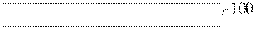
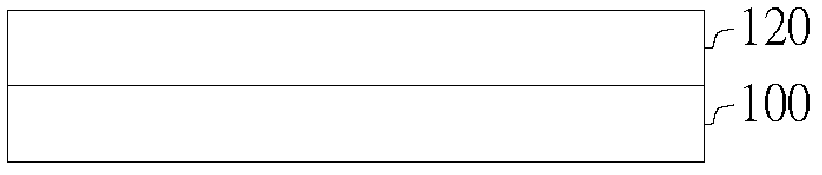
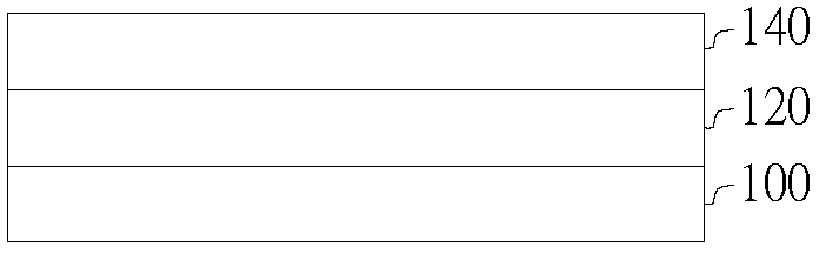
[0031] Please refer to Figure 1A ~ Figure 1D , which shows a schematic diagram of the manufacturing process of the first conductive layer M1 according to an embodiment of the present invention. Such as Figure 1A As shown, a substrate 100 is provided, and the material of the substrate 100 is, for example, polyethylene terephthalate (PET), polyethylene naphthalate (PEN), triacetate cellulose (TriacetateCellulose, TAC), polycarbonate Ester (Polycarbonate, PC) or polyimide (Polyimide, PI). Next, if Figure 1B As shown, a barrier layer (barrier layer) 120 is formed on the substrate 100, for example, the barrier layer 120 is formed by silicon oxide (SiO X ), alumina (AlO X ) or zinc oxide (ZnO) is deposited on the substrate 100. The thickness of the barrier layer 120 is, for example, 10 nanometers (nm) to 1000 nm. Of course, as long as the barrier layer 120 can avoid the formation of the conductive layer after the substrate 100 is affected by the gas released during the manu...

no. 2 example

[0044] Please refer to Figure 2A ~ Figure 2C , which shows a schematic diagram of the manufacturing process of the second conductive layer M2 according to another embodiment of the present invention. Such as Figure 2A As shown, a substrate 200 is provided. The material of the substrate 200 is, for example, the same as that of the substrate 100 of the first embodiment, and a barrier layer 220 is formed on the substrate 200. The material, thickness and formation method of the barrier layer 220 are the same as those of the barrier layer 120. Moreover, the structure of the barrier layer 220 can be omitted according to the requirements of the manufacturing process.

[0045] Please refer to Figure 2B , forming a conductive material layer 240 on the barrier layer 220 . In this embodiment, the conductive material layer 240 is formed by, for example, depositing indium tin oxide (ITO) on the barrier layer 220 by roll-to-roll physical vapor deposition. Next, please refer to Figu...


PUM

PropertyMeasurementUnit
thicknessaaaaaaaaaa
thicknessaaaaaaaaaa
thicknessaaaaaaaaaa

Abstract

The invention discloses a composite conductive structure which comprises a first substrate and a first conductive layer. The first conductive layer is arranged on the first substrate, and the first conductive layer comprises a crystalline-state conductive film and a non-crystalline-state conductive film. The invention further discloses a manufacturing method of the composite conductive structure and a display and touch panel with the composite conductive structure. The composite conductive structure and the manufacturing method of the composite conductive structure can improve the situation that after the conductive layer is bent, disconnection is prone to occurring. Moreover, a display device manufactured by the application of the conductive layer can avoid the problem that circuit disconnection occurs after the conductive layer is bent or driving resistance becomes larger, and the durability and sensitivity of the display device are both expected to be improved.

Description

technical field [0001] The present invention relates to a composite conductive structure, a method for manufacturing the composite conductive structure, and a touch panel and a display panel with the composite conductive structure, and in particular to a composite conductive film with a crystalline conductive film and an amorphous conductive film Composite conductive structure and touch panel and display panel with such composite conductive structure. Background technique [0002] With the advancement of technology, our daily life has been filled with all kinds of monitors. The application of displays is becoming more and more common, so that the development of each component in the display becomes the research goal of manufacturers. Among them, the flexible components used in displays have become a popular research and development subject along with the development of flexible displays. Flexible display panels or display panels requiring impact resistance usually use flex...

Claims


Application Information

Patent Timeline
Patent Type & Authority Applications(China)
IPC IPC(8): H01B5/14H01B13/00G06F3/041
Inventor 庄闵超许育纯赖思维
Owner INNOCOM TECH SHENZHEN
Why Eureka
Try Eureka