Groove-type silicon nanocrystalline memory and manufacturing method thereof

A silicon nanocrystal and memory technology, which is applied in the field of memory, can solve problems such as deterioration of device storage characteristics, achieve changes in erasure characteristics, avoid increased edge thickness, and simple methods

Active Publication Date: 2013-09-11
INST OF MICROELECTRONICS CHINESE ACAD OF SCI
View PDF4 Cites 0 Cited by
  • Summary
  • Abstract
  • Description
  • Claims
  • Application Information

AI Technical Summary

Problems solved by technology

In this way, when making the gate oxide layer of peripheral devices, under high temperature conditions, oxygen or water molecules will quickly migrate into the middle of the device along the tunnel oxide layer and inter-gate oxide layer of the silicon nanocrystal storage unit, resulting in the oxidation of the silicon nanocrystal , so the tunneling oxide layer at the edge of the device will also thicken, and the storage characteristics of the final device will deteriorate, that is, the traditional silicon nanocrystal device will be affected by the smiling effect during the fabrication process, such as figure 1 shown

Method used


Image

  • Groove-type silicon nanocrystalline memory and manufacturing method thereof
  • Groove-type silicon nanocrystalline memory and manufacturing method thereof
  • Groove-type silicon nanocrystalline memory and manufacturing method thereof

Examples


Embodiment Construction

[0021] In order to make the object, technical solution and advantages of the present invention clearer, the present invention will be described in further detail below in conjunction with specific embodiments and with reference to the accompanying drawings.

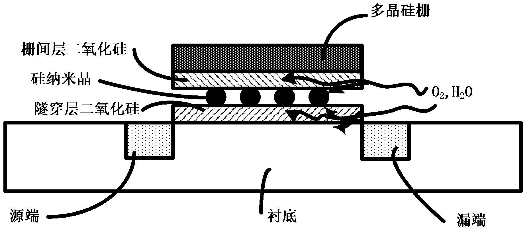
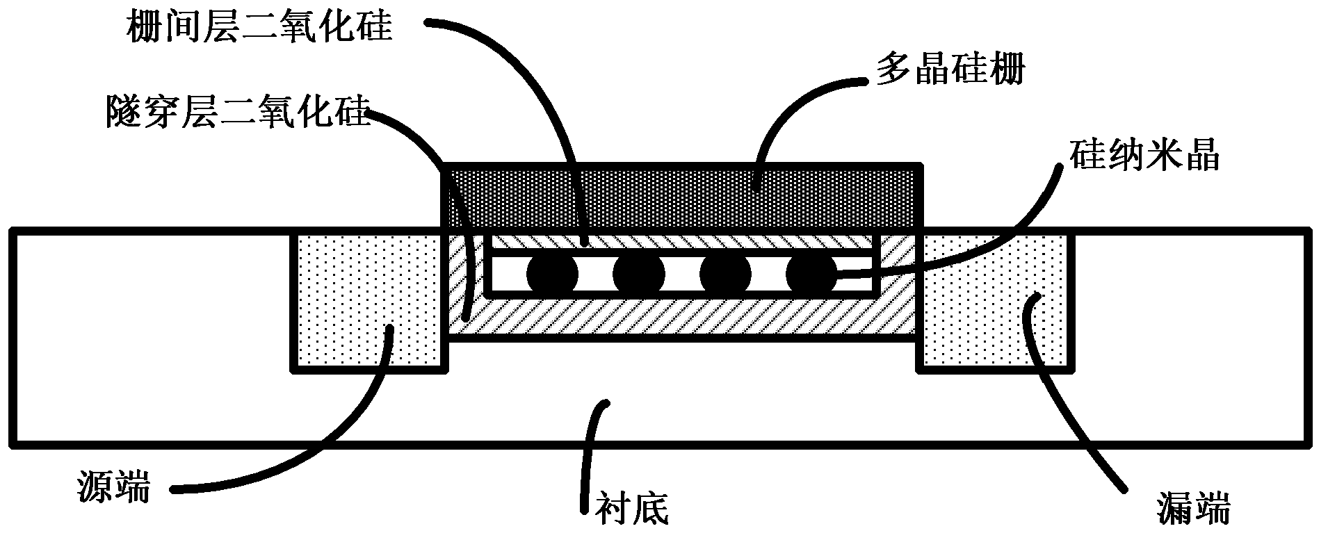
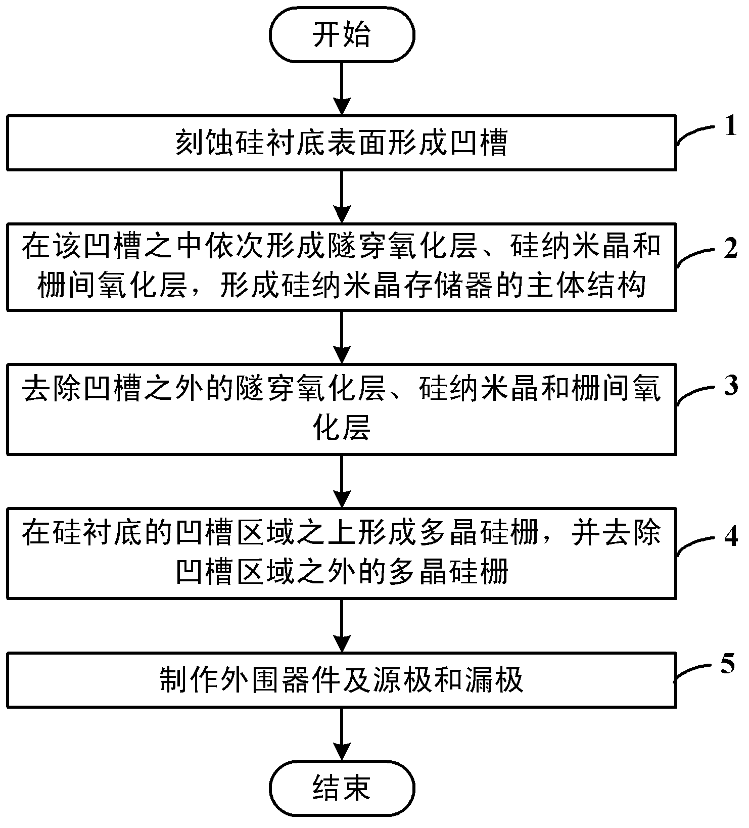
[0022] Aiming at how to thoroughly avoid the influence of the smiling face effect on silicon nanocrystal devices, the present invention adopts a grooved silicon nanocrystal device structure, so that silicon nanocrystals, tunnel oxide layers, and inter-gate oxide layers are located in the grooves, and the upper Covering the polysilicon gate, so that the silicon nanocrystals are not oxidized, and the thickness of the edge of the tunnel oxide layer will not increase, so the storage window of the device with this structure is large and the uniformity is better.

[0023] The silicon nanocrystal storage device structure provided by the invention is realized by fabricating a device on a groove on a silicon substrate. The groove i...


PUM

PropertyMeasurementUnit
depthaaaaaaaaaa
thicknessaaaaaaaaaa
thicknessaaaaaaaaaa

Abstract

The invention discloses a groove-type silicon nanocrystalline memory and a manufacturing method thereof. The groove-type silicon nanocrystalline memory comprises a groove formed in the surface of an etching silicon substrate, a main structure of the silicon nanocrystalline memory formed in the groove, a polysilicon gate covered above the groove of the silicon substrate, and a source electrode and a drain electrode formed in the silicon substrate on two sides of the groove, and the main structure comprises a tunneling oxidation layer, silicon nanocrystalline and an inter-gate oxidation layer sequentially from bottom to top. According to the manufacturing method, the groove-type silicon nanocrystalline memory can be manufactured only by etching the groove on the substrate and manufacturing devices on the groove, so that the method is simple; the manufacturing method is completely compatible with conventional CMOS (complementary metal oxide semiconductor) processes, and the devices are good in storage characteristic and high in reliability and quite suitable for large-scale production and wide application; smiling effect in the process of manufacturing of peripheral devices can be thoroughly avoided from oxidizing the silicon nanocrystalline, so that storage characteristics and the like of the devices are guaranteed.

Description

technical field [0001] The invention relates to the technical field of memory, in particular to a grooved silicon nanocrystal memory and a manufacturing method thereof. Background technique [0002] With the continuous advancement of microelectronics process nodes, the traditional flash memory technology based on polysilicon floating gates is facing serious technical difficulties. The most important problem is that the contradiction between device size miniaturization and device reliability cannot be effectively resolved. . To solve this contradiction, S.Tiwari proposed silicon nanocrystal memory based on discrete storage in 1996. This kind of memory has the advantages of fast erasing and writing speed, high reliability, simple manufacturing process, low cost, and full compatibility with traditional CMOS technology. Volatile memory. [0003] However, there are also problems in process integration for silicon nanocrystal floating gate memory, especially the existence of hi...

Claims


Application Information

Patent Timeline
Patent Type & Authority Applications(China)
IPC IPC(8): H01L27/115H01L29/06H01L21/8247
Inventor 王永刘明霍宗亮刘璟张满红张康玮
Owner INST OF MICROELECTRONICS CHINESE ACAD OF SCI
Why Eureka
Try Eureka