Electroplating method for PCB plate and apparatus

A PCB board and electroplating device technology, applied in the field of PCB board electroplating methods and devices, can solve problems such as inability to guarantee the exchange effect of PCB electroplating solution, insufficient thickness of the electroplating layer in holes, and low flow of electroplating solution, etc., so as to improve deep plating ability , Uniform thickness and full flow effect

Active Publication Date: 2013-09-18
SHENNAN CIRCUITS
View PDF4 Cites 19 Cited by
  • Summary
  • Abstract
  • Description
  • Claims
  • Application Information

AI Technical Summary

Problems solved by technology

[0002] In the process of PCB board processing, the electroplating method usually used is a continuous fully automatic spraying method, such as the invention patent with the application number CN200610061541.0, which uses the method of bottom spraying, that is, spraying is set under both sides of the PCB board The direction is parallel to the nozzle of the PCB board surface, and the electroplating solution is sprayed out through the nozzle parallel to the PCB board surface. This method can improve the exchange of the electroplating solut

Method used


Image

  • Electroplating method for PCB plate and apparatus
  • Electroplating method for PCB plate and apparatus
  • Electroplating method for PCB plate and apparatus

Examples


Example Embodiment

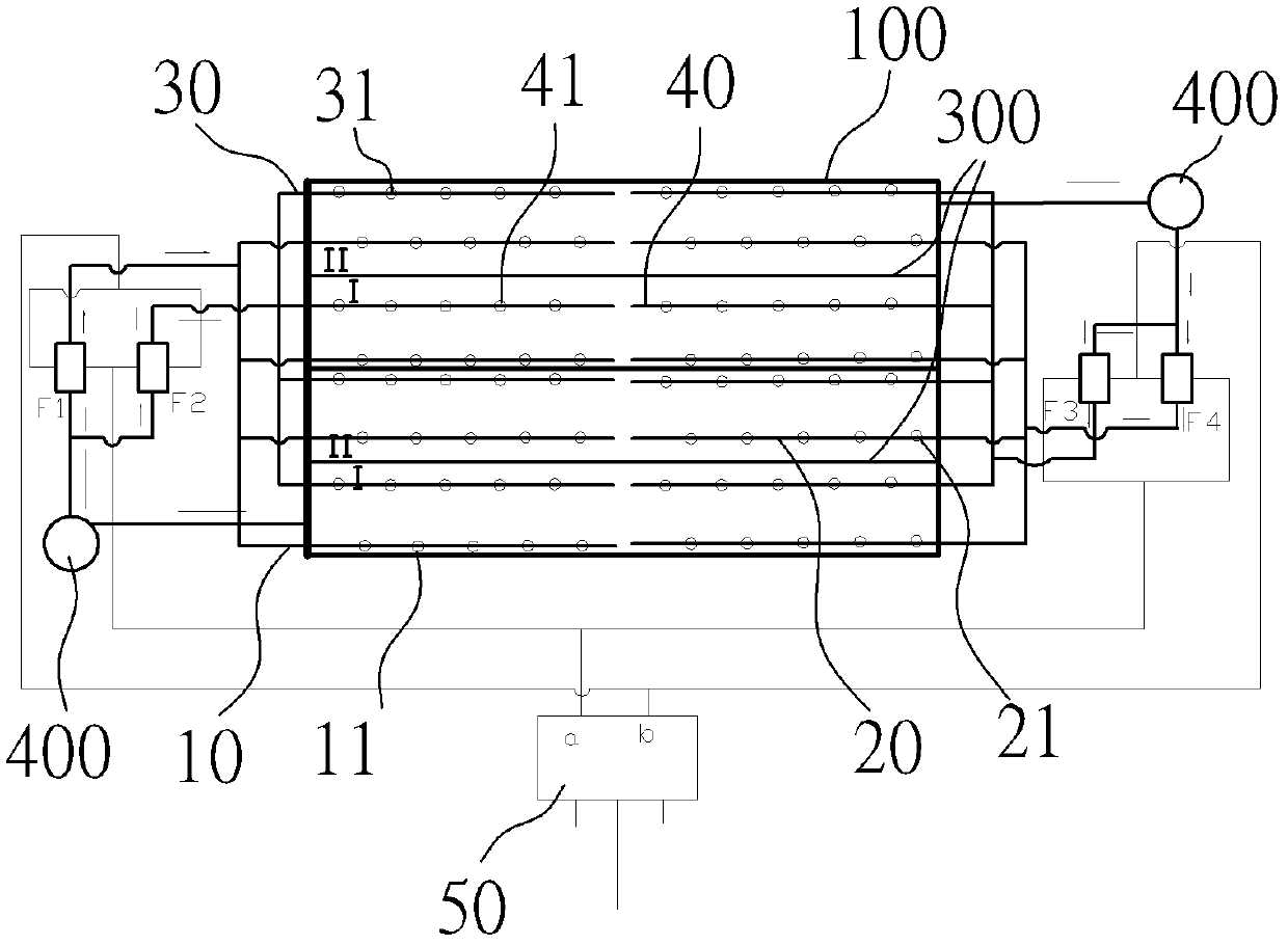
[0012] Please refer to Figure 1~Figure 2 , The PCB board electroplating device of the embodiment of the present invention can alternately perform side spray on both sides of the PCB board 200, and perform side spray on one board surface while performing bottom spray on the other board surface. The electroplating solution forms turbulent flow. The two sides of the hole of the PCB board produce large negative pressure due to the different flow rate of the electroplating solution. The flow effect of the electroplating solution in the hole is sufficient, the exchange capacity is strong, and the deposition speed of copper ions is fast, which improves the deep plating ability and makes The thickness of the electroplated copper in the hole is sufficient and uniform.

[0013] The PCB board electroplating device includes an electroplating tank 100 and a holding assembly 300 for holding the PCB board 200 immersed in the electroplating solution in the electroplating tank 100. The electropl...


PUM


Abstract

The invention discloses an electroplating method for a PCB plate and an apparatus. The method comprises: a preparation step comprising immersing the PCB plate in a plating solution of a plating bath in a way that a plate surface is perpendicular to a liquid surface, wherein a first side of the PCB plate has a first side nozzle set and a second bottom nozzle set, and a second side of the PCB plate has a second side nozzle set and a first bottom nozzle set; and a jet flow processing step, wherein a first nozzle group composed of the first side nozzle set and the first bottom nozzle set and a second nozzle group composed of the second side nozzle set and the second bottom nozzle set cyclically and alternately jet for predetermined times. The electroplating method for the PCB plate and the apparatus provided by the invention utilize a technical means that two nozzle groups cyclically and alternately jet. A relatively large negative pressure is generated at two sides of the holes of the PCB plate due to different flow rates of the plating solution. A flow effect of the plating solution is relatively full, an exchange capability is relatively strong, and a deposition speed of copper ions is increased, thereby improving a throwing power so that a thickness of electro-coppering is enough and uniform.

Description

technical field [0001] The invention relates to the field of PCB board manufacturing, in particular to a PCB board electroplating method and device. Background technique [0002] In the process of PCB board processing, the electroplating method usually used is a continuous fully automatic spraying method, such as the invention patent with the application number CN200610061541.0, which uses the method of bottom spraying, that is, spraying is set under both sides of the PCB board The direction is parallel to the nozzle of the PCB board surface, and the electroplating solution is sprayed out through the nozzle parallel to the PCB board surface. This method can improve the exchange of the electroplating solution in the hole of the high-thickness-diameter ratio PCB to a certain extent, but there are still problems. The negative pressure is small, and the flow rate of the plating solution in the hole is small. With the gradual increase of the thickness-to-diameter ratio, especiall...

Claims


Application Information

Patent Timeline
IPC IPC(8): C25D5/08H05K3/18
Inventor 陈于春黄蕾刘玉涛卢利斌管育时沙雷
Owner SHENNAN CIRCUITS
Why Eureka
Try Eureka