Eureka AIR delivers breakthrough ideas for toughest innovation challenges, trusted by R&D personnel around the world.

Method for preventing lateral undercutting of micro-convex points in manufacturing process of micro-convex points

A manufacturing process and micro-bump technology, which is applied in semiconductor/solid-state device manufacturing, electrical components, electrical solid-state devices, etc., can solve problems such as control limitations of etching processes, improve reliability and yield, and prevent lateral The effect of undercutting

Active Publication Date: 2013-09-18
NAT CENT FOR ADVANCED PACKAGING
View PDF11 Cites 9 Cited by
  • Summary
  • Abstract
  • Description
  • Claims
  • Application Information

AI Technical Summary

Problems solved by technology

Due to the problem of undercutting, the selection of etching solution and the control of etching process will be limited when etching the seed layer

Method used


Image

  • Method for preventing lateral undercutting of micro-convex points in manufacturing process of micro-convex points
  • Method for preventing lateral undercutting of micro-convex points in manufacturing process of micro-convex points
  • Method for preventing lateral undercutting of micro-convex points in manufacturing process of micro-convex points

Examples


Embodiment Construction

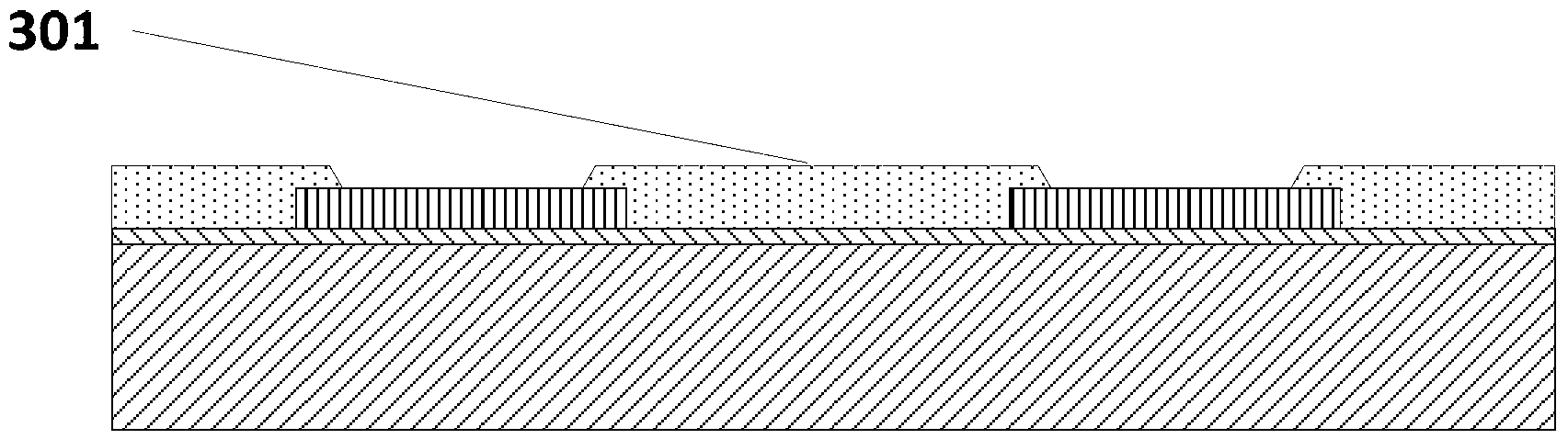
[0031] The present invention proposes to cover a layer of etching barrier layer on the seed layer around the micro-bump, so that when the seed layer is etched, the seed layer below it can be protected from etching, thereby preventing the occurrence of side undercutting. Phenomenon.

[0032] Specifically, the embodiment of the present invention discloses a method for forming micro-bumps, including:

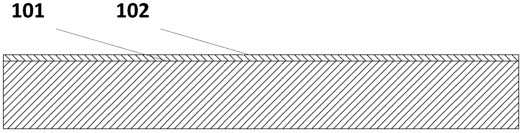
[0033] s1, forming a pad on the semiconductor substrate;

[0034] s2. A dielectric layer is formed on the pad and the surface of the semiconductor substrate, and a window is opened on the dielectric layer, and the window corresponds to the pad;

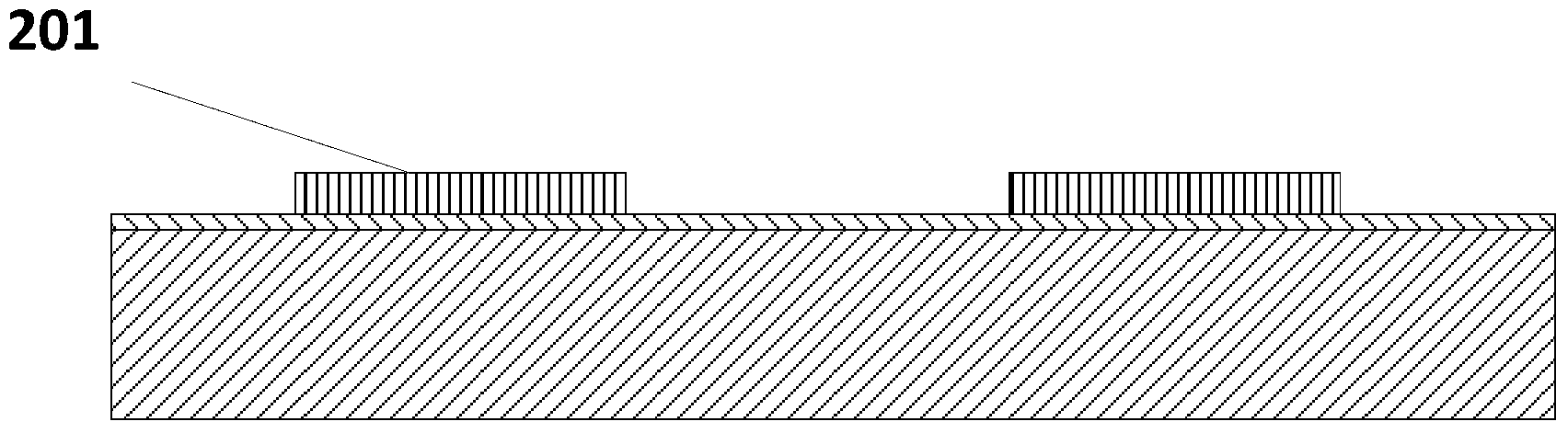
[0035] s3, forming a seed layer on the surface of the dielectric layer and the pad;

[0036] s4, electroplating on the surface of the seed layer to form micro-bumps;

[0037] s5, forming a barrier layer on the seed layer within a certain distance around the micro-bump, the certain distance satisfies: after the etching in step s6, the en...


PUM


Abstract

The invention discloses a forming method of micro-convex points. The forming method comprises the following steps of s1, forming a welding disc on a semiconductor substrate; s2, forming a medium layer on the surfaces of the welding disc and the semiconductor substrate, wherein the medium layer is provided with a window which corresponds to the welding disc; s3, forming a seed layer on the surfaces of the medium layer and the welding disc; s4, forming the micro-convex points on the surface of the seed layer in an electroplating manner; s5, forming a blocking layer on the seed layer around the micro-convex points within a certain distance; s6, etching the seed layer which is not covered by the blocking layer; and s7, returning welding flux. The method disclosed by the invention has the advantages that since an etching blocking layer covers the seed layer around the micro-convex points, when the seed layer is etched, the seed layer under the etching blocking layer can be protected from being etched, so that the phenomenon of lateral undercutting is prevented; and the reliability and the yield of processing and manufacturing of the micro-convex points are improved.

Description

technical field [0001] The invention belongs to the technical field of semiconductor manufacturing, in particular to a method for preventing lateral undercutting of micro bumps during the manufacturing process of micro bumps. Background technique [0002] Traditionally, the electrical connection between the IC chip and the outside is achieved by bonding the I / O on the chip to the package carrier with metal leads and through the package pins. With the reduction of IC chip feature size and the expansion of integration scale, the distance between I / O is decreasing and the number is increasing. When the I / O pitch is reduced below 70 μm, the wire bonding technology is no longer applicable, and new technical approaches must be sought. [0003] Wafer-level packaging technology uses thin film redistribution technology, so that I / O can be distributed on the entire surface of the IC, instead of being limited to the peripheral area of ​​the narrow IC chip, thus solving the problem of ...

Claims


Application Information

Patent Timeline
Patent Type & Authority Applications(China)
IPC IPC(8): H01L21/48H01L21/60
CPCH01L24/11H01L2224/03622H01L2224/10126H01L2224/11H01L2224/11009H01L2924/00012
Inventor 戴风伟张文奇于大全
Owner NAT CENT FOR ADVANCED PACKAGING
Why Eureka
Eureka Blog
Learn More