Check patentability & draft patents in minutes with Patsnap Eureka AI!

Chip stack structure and method for fabricating the same

A technology of chip stacking and manufacturing method, applied in the fields of semiconductor/solid-state device manufacturing, electrical components, electrical solid-state devices, etc., can solve the problems affecting the overall product reliability, high structural residual stress, affecting the processing yield, etc., to shorten the processing time. Time, reduced processing cost, simple processing effect

Active Publication Date: 2013-09-18
IND TECH RES INST
View PDF3 Cites 8 Cited by
  • Summary
  • Abstract
  • Description
  • Claims
  • Application Information

AI Technical Summary

Problems solved by technology

For example: the temperature of the joining process is higher, which may cause higher structural residual stress
When performing high-density chip packaging, due to the narrow cutting line, it is not conducive to the subsequent dispensing process
In addition, the module still needs to be molded after the dispensing of glue, but because the existing chip stacking is to temporarily attach the large wafer to the carrier through the glue material, and then stack the chips on the large wafer, Therefore, when the molding is completed and debonding is performed, some adhesive material will remain on the bumps, affecting the processing yield
In addition, the bonding interface between the packaging module and the external intermediary substrate or circuit substrate is easily damaged, which affects the reliability of the overall product

Method used


Image

  • Chip stack structure and method for fabricating the same
  • Chip stack structure and method for fabricating the same
  • Chip stack structure and method for fabricating the same

Examples


Embodiment Construction

[0110] Below in conjunction with accompanying drawing, structural principle and working principle of the present invention are specifically described:

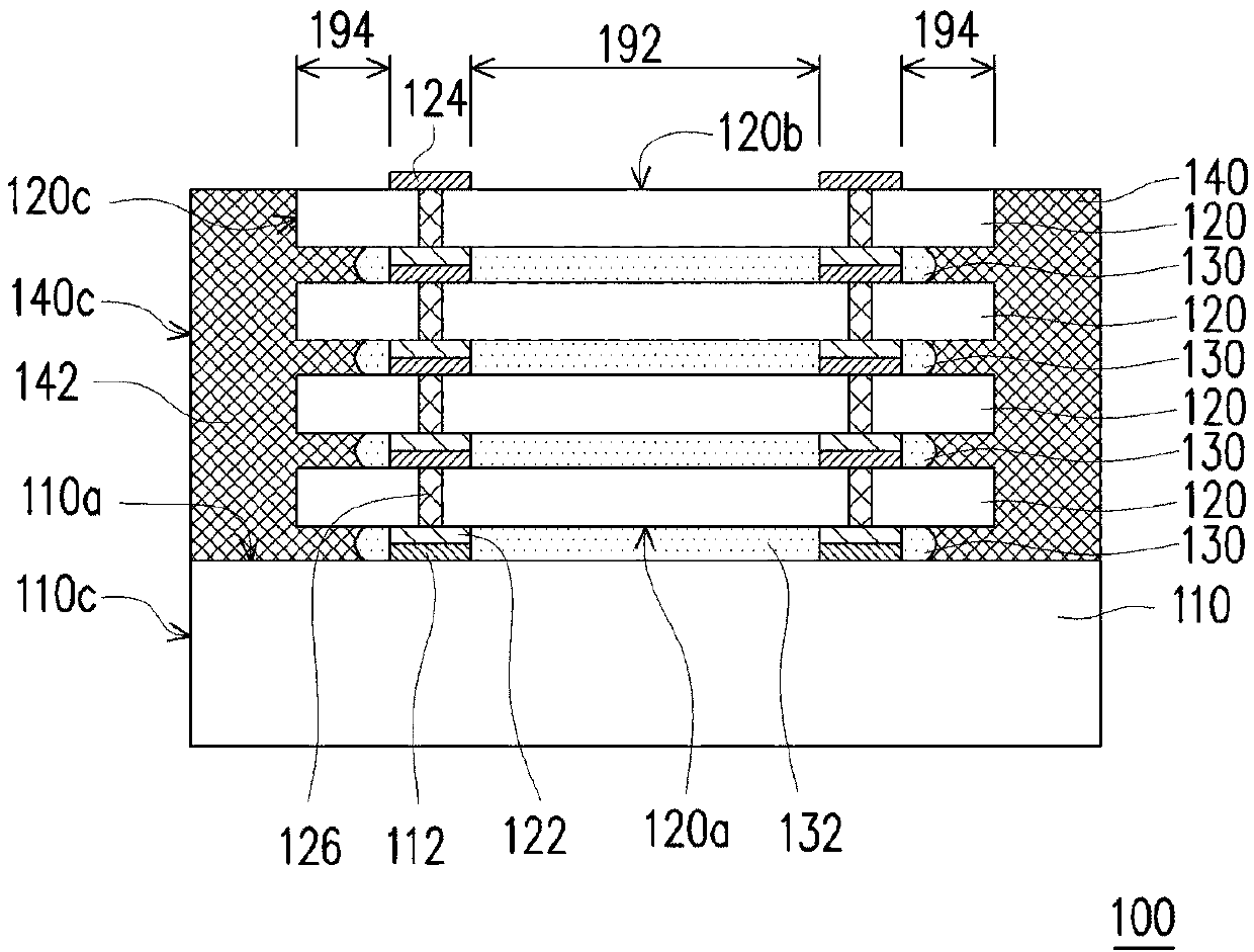
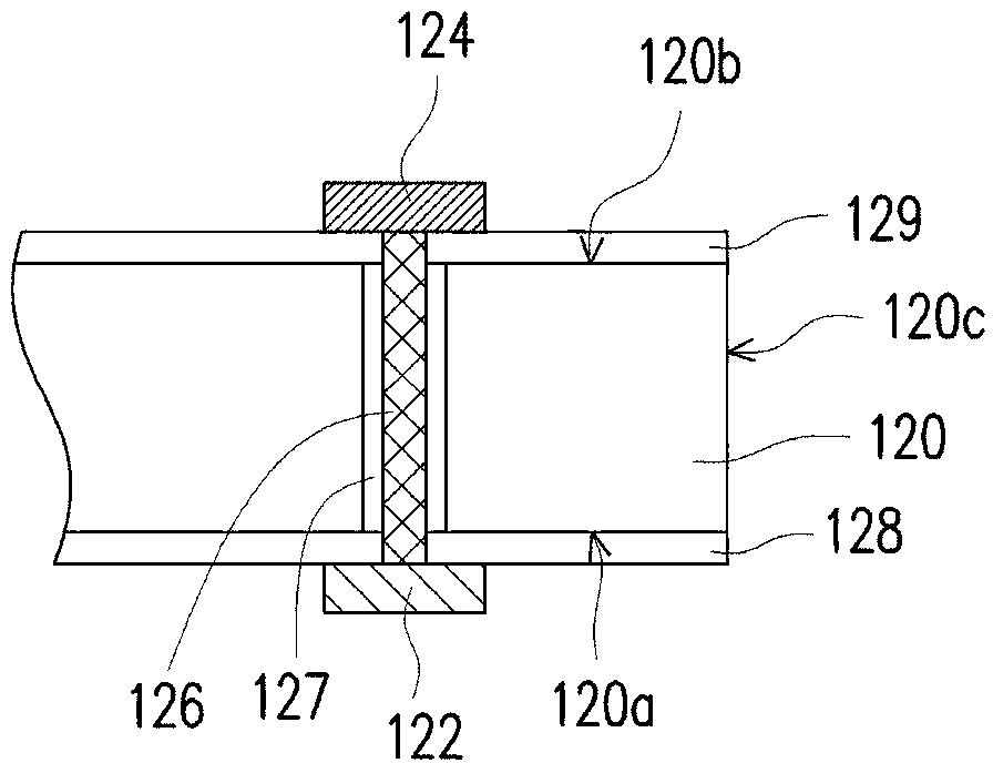
[0111] Figure 1A It is a chip stack structure according to an embodiment of the present invention. The chip stacking structure 100 of this embodiment is directly stacking chips on a large wafer, and the formed structure includes a first chip 110 as a stacking base, and one or more second chips 120 stacked on the first chip 110, The thickness of the first chip 110 is greater than 100 microns (μm), which can provide good support during processing. In addition, the size of the first chip 110 is, for example, larger than the size of the second chip 120 , wherein the size refers to parameters such as thickness, length, width, and area of ​​the chip.

[0112] This embodiment is a case of stacking a plurality of second chips 120 , however, the number of second chips 120 can be changed according to actual needs, and is not limited t...


PUM


Abstract

A chip stack structure taking a wafer as a stacking base and stacking chips thereon is provided. The chip stack structure is capable of achieving high density electrode bonding and breaking the bottleneck of requiring interposer to serve as a transferring interface in three dimensional chip package. The chip stack structure is easily fabricated and compatible with wafer level process, so as to reduce processing time and manufacturing cost. A method for fabricating the chip stack structure is also provided.

Description

technical field [0001] The invention relates to a semiconductor technology, in particular to a chip stacking structure and a manufacturing method thereof. Background technique [0002] In today's information society, the design of electronic products is developing towards the trend of light, thin, short and small. The use of three-dimensional chip integration technology can realize high-density chip construction, and has the advantages of high efficiency and low energy consumption. For example, in the field of portable electronic products that emphasize multi-function and small size, including Solid State Disk / Drive (SSD) or Dynamic Random Access Memory (DRAM), etc., in addition to enhancing high-speed performance, it can also be used in With the same number of I / Os, the power loss required for chip operation is reduced, and at the same time, the requirements for capacity, performance and I / O improvement are met. [0003] The stacking process used in the current 3D chip in...

Claims


Application Information

Patent Timeline
Patent Type & Authority Applications(China)
IPC IPC(8): H01L25/065H01L21/31H01L21/98
CPCH01L24/94H01L24/96H01L24/97H01L25/0657H01L25/50H01L2224/0401H01L2224/04105H01L2224/12105H01L2224/16145H01L2224/16225H01L2224/32145H01L2224/32225H01L2224/73204H01L2224/73259H01L2224/94H01L2224/97H01L2225/06513H01L2225/06517H01L2225/06541H01L2225/06565H01L2225/06568H01L2924/15311H01L2224/81H01L2924/00012H01L2924/00
Inventor 陆苏财庄敬业
Owner IND TECH RES INST
Features
  • R&D
  • Intellectual Property
  • Life Sciences
  • Materials
  • Tech Scout
  • Unparalleled Data Quality
  • Higher Quality Content
  • 60% Fewer Hallucinations
Learn More