Method for detecting DNA mutation based on graphene sensor
A graphene and sensor technology, applied in the field of biology, can solve problems such as sensitivity and specificity limitations, and achieve the effect of high specificity and good stability
- Summary
- Abstract
- Description
- Claims
- Application Information
AI Technical Summary
Problems solved by technology
Method used
Image
Examples
Embodiment 1
[0017] Example 1: Detection of DNA methylation based on graphene sensors
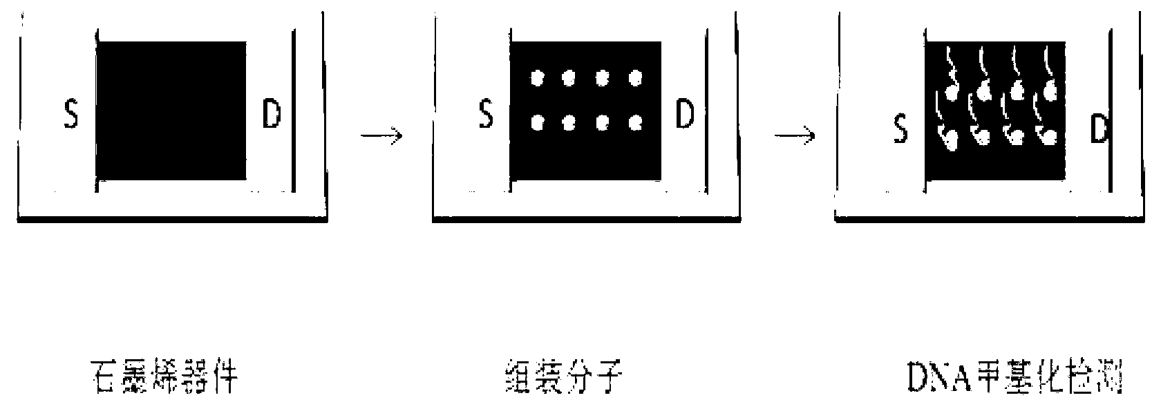
[0018] For the entire testing process, see figure 1 , first prepare a graphene device with electrodes at both ends, S is the source, D is the drain, assemble the connecting molecules on the graphene surface of the graphene device, connect the DNA to the graphene surface, and perform related detection.
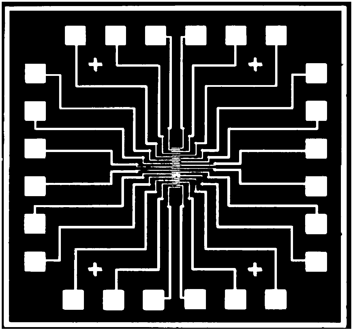
[0019] 1) Preparation of device: a) Use a flexible polymethyl methacrylate (PMMA) polymer film as a support, spin-coat PMMA film on the copper foil with grown graphene, bake at 180°C for 2min, and then place the sample Placed in a saturated ferric nitrate solution, the copper foil is etched away, and the graphene embedded in the PMMA film is separated. The PMMA film carrying the graphene film can be attached to the silicon substrate, and then the PMMA film can be removed with acetone.
[0020] b) Spin-coat photoresist on the graphene, denote as photoresist 1, expose photoresist 1 to obtain a mark patte...
Embodiment 2
[0027] Embodiment 2: Detect SNP based on graphene sensor
[0028] 1) Preparation of device: a) Use a flexible polymethyl methacrylate (PMMA) polymer film as a support, spin-coat PMMA film on the copper foil with grown graphene, bake at 180°C for 2min, and then place the sample Placed in a saturated ferric nitrate solution, the copper foil is etched away, and the graphene embedded in the PMMA film is separated. The PMMA film carrying the graphene film can be attached to the silicon substrate, and then the PMMA film can be removed with acetone.
[0029] b) Spin-coat photoresist on the graphene, denote as photoresist 1, expose photoresist 1 to obtain a mark pattern, and vapor-deposit a thickness of 1-100nm (such as 80nm) Cr layer, 20 -1000nm (as 200nm) Au layer, remove the photoresist 1, left the vapor-deposited metal mark at the graphene exposure position, and the metal mark is used for the position alignment mark of next two steps photolithography; Wherein, the The graphene i...
PUM
| Property | Measurement | Unit |
|---|---|---|
| Thickness | aaaaa | aaaaa |
| Thickness | aaaaa | aaaaa |
Abstract
Description
Claims
Application Information


