TSV (through silicon via) Trench arrangement method in 3D integrated circuit

A technology of integrated circuits and layout methods, applied in the field of automatic layout, to meet the requirements of process spacing constraints and achieve the effect of compact layout

Inactive Publication Date: 2013-09-25
BEIJING UNIV OF TECH
View PDF3 Cites 10 Cited by
  • Summary
  • Abstract
  • Description
  • Claims
  • Application Information

AI Technical Summary

Problems solved by technology

[0004] Unfortunately, there is currently no method for the automatic design of 3D integrated circuits with respect to TSV positioning. Therefore, it is necessary to be able to propose an automatic design method for 3D integrated circuits

Method used


Image

  • TSV (through silicon via) Trench arrangement method in 3D integrated circuit
  • TSV (through silicon via) Trench arrangement method in 3D integrated circuit
  • TSV (through silicon via) Trench arrangement method in 3D integrated circuit

Examples


Embodiment Construction

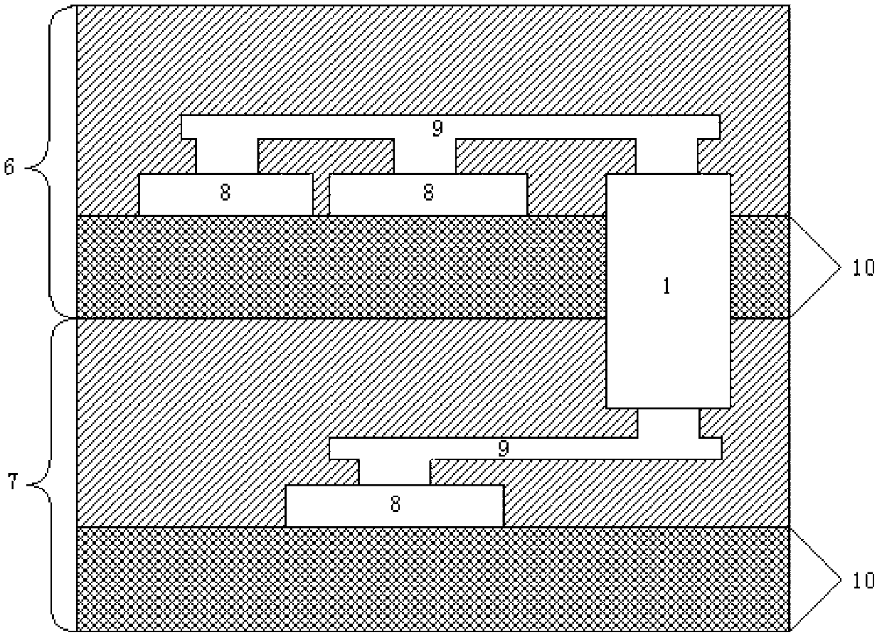
[0044] A schematic diagram of the structure of a 3D integrated circuit such as figure 1 shown. A 3D circuit is a structure in which multi-layer 2D chips are stacked in the vertical direction, and the structural relationship between any two layers of adjacent chips is as follows: figure 1 The top chip 6 and the bottom chip 7, the standard unit 8 in the chip is the basic structure for the storage and transmission of integrated circuit signals, and the metal interconnection line 9 connects the standard unit to complete the interconnection on the single-layer chip. TSV1 interconnection is used for cross-layer interconnection of standard cells to complete cross-layer transmission of signals. The structure of TSV1 is a via hole passing through two adjacent layers of the 3D integrated circuit chip.

[0045] The present invention is dedicated to optimizing the layout where TSV positions have been preliminarily determined, so that the spacing of all TSVs meets the requirements of the...


PUM


Abstract

A TSV (through silicon via) Trench arrangement method in a 3D integrated circuit belongs to the field of 3D integrated circuit design. During the machining production of the 3D integrated circuit, a TSV layout is optimized in a Trench with a single-layered layout to facilitate the machining of TSVs. According to the invention, positions and distances of TSVs can be optimized through the grid method, so that the layout is optimized, the TSVs are placed in the Trench with the single-layered layout, the distance of the TSVs meets the requirement for technological machining, and the manufacture is completed. The realizing method provided by the invention includes the following steps: firstly forming a rectangular coordinate system in a TSV originally positioned layout; confirming coordinates of TSVs; generating a grid and guaranteeing that the distance of every two grid points in the grid is larger than the minimum technologically machinable distance; moving each TSV to the grid point nearest to the TSV; finally disposing the situation that a plurality of TSVs are arranged at a single point, so as to guarantee that only one TSV is arranged on each grid point in the final layout, and completing the optimization, machining and manufacturing the integrated circuit.

Description

technical field [0001] The present invention relates to the field of design and manufacture of 3D integrated circuits, and more specifically, the present invention relates to an automatic layout method used in the design of three-dimensional integrated circuits. Background technique [0002] The design and manufacturing level of integrated circuits has been developing rapidly, and now hundreds of millions of transistors can be integrated on a single chip. More specifically, according to the description of Moore's Law, the advanced technology level has reached the nanometer level. Due to the increase in the number of transistors on a single chip, ordinary 2D integrated circuits will cause the problem of excessively long lines, which will reduce the operation speed of the circuit and increase power consumption. The 3D integrated circuit can effectively reduce the length of the line, improve the speed of operation, and reduce power consumption. [0003] 3D integrated circuits...

Claims


Application Information

Patent Timeline
Patent Type & Authority Applications(China)
IPC IPC(8): G06F17/50
Inventor 侯立刚汪金辉路博白澍彭晓宏耿淑琴
Owner BEIJING UNIV OF TECH
Why Eureka
Try Eureka