Built-in endurance test system, aging test device and corresponding endurance testing method

A test system and aging test technology, applied in the field of charge pump, can solve the problems of inability to automatically judge the failure of chip sample reading kinetic energy, the number of endurance test samples is small, and the endurance test cycle is long, so as to save endurance test cycle, simple packaging, The effect of saving packaging costs

Active Publication Date: 2013-10-02
SHANGHAI HUAHONG GRACE SEMICON MFG CORP
View PDF6 Cites 6 Cited by
  • Summary
  • Abstract
  • Description
  • Claims
  • Application Information

AI Technical Summary

Problems solved by technology

[0008] The purpose of the present invention is to provide a built-in endurance test system, an aging test device and a corresponding endurance test method to solve the problem that the number of endurance test sa

Method used


Image

  • Built-in endurance test system, aging test device and corresponding endurance testing method
  • Built-in endurance test system, aging test device and corresponding endurance testing method
  • Built-in endurance test system, aging test device and corresponding endurance testing method

Examples


Embodiment 1

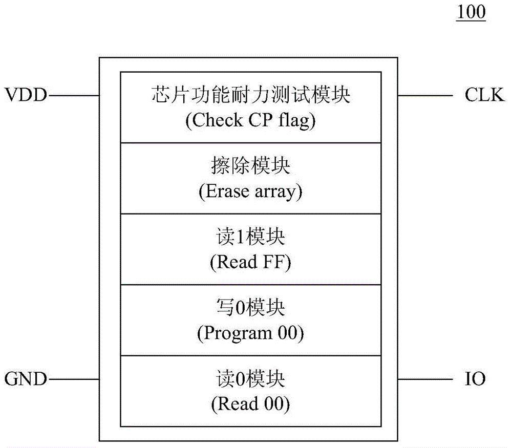
[0060] see figure 1 , to describe in detail a built-in endurance test system provided by the present invention. The built-in endurance test system 100 includes a power supply terminal VDD, a ground terminal GND, a clock terminal CLK and an output terminal IO, when the power supply terminal of the built-in endurance test system receives the power supply, the ground terminal receives the ground voltage and When the clock terminal receives the clock signal, the built-in endurance test system starts to perform endurance test on the chip with the built-in endurance test system, and outputs the endurance test result of the chip through the output terminal of the built-in endurance test system. The built-in endurance test system only needs to be packaged with 4 ports. Compared with the traditional endurance test system with an external chip, the package is simple and the package cost is saved.

[0061] Further, the endurance test performed on the chip by the built-in endurance test ...

Embodiment 2

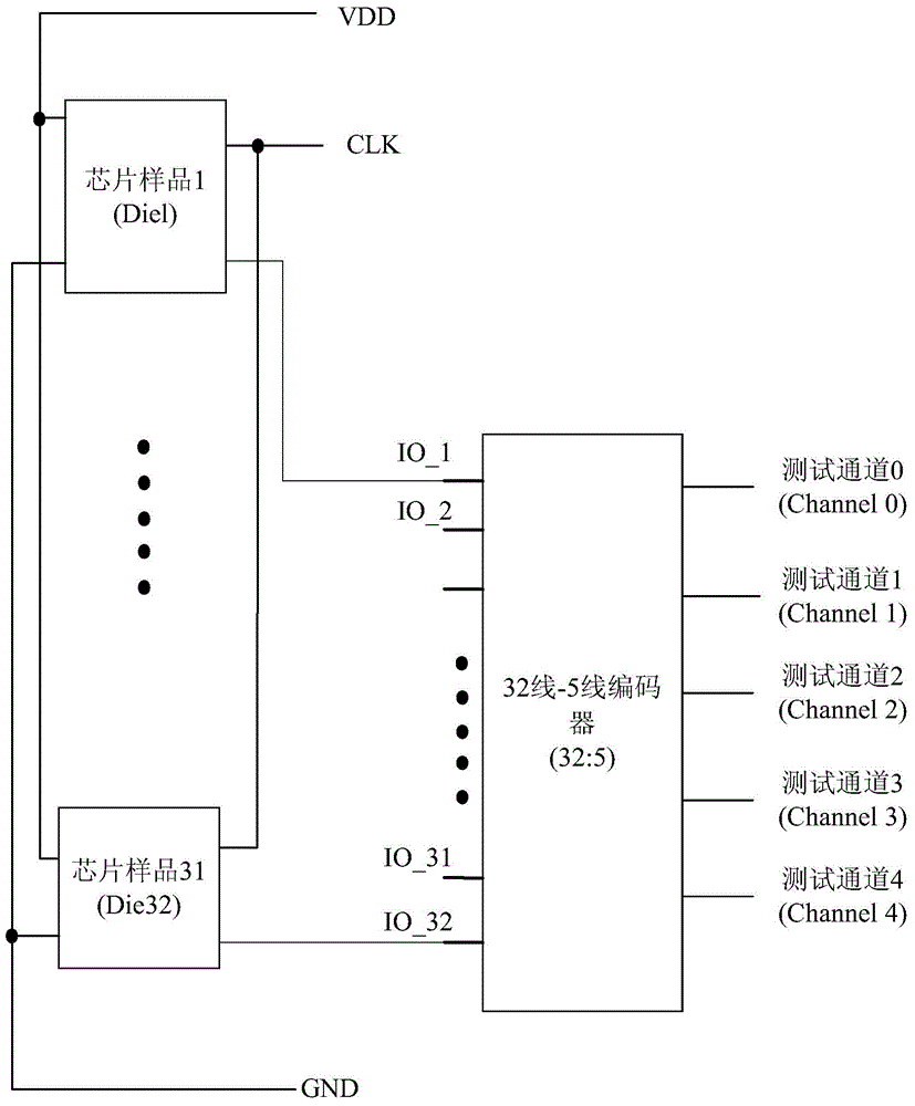
[0064] see figure 2 , a detailed description of an aging test device provided by the present invention. The burn-in test device includes a complete machine test board (FT board), at least one group of chips, multiple built-in endurance test systems 100 , at least one decoder 200 and a terminal test device 300 .

[0065] Since a maximum of 3000 chips can be installed on the complete machine test board at one time, its price is not only cheaper than that of the semiconductor aging test board, but also much more than the number of chips placed on the semiconductor aging test board.

[0066] Specifically, each chip in each group of chips is placed on the complete machine test board. The built-in endurance test system of the present invention is integrated in each chip (the built-in endurance test system does not include a counter), and the power supply terminals in each of the built-in endurance test systems are connected together. The ground terminals of the built-in endurance...

Embodiment 3

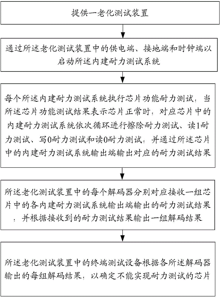
[0086] by image 3 The flow chart shown is taken as an example to describe in detail an endurance testing method of the present invention. Described endurance test method comprises the steps:

[0087] In step 1, the aging test device of the present invention is provided.

[0088] In step 2, the built-in endurance test system is activated through the power supply terminal, the ground terminal and the clock terminal in the aging test device.

[0089] In step 3, each of the built-in endurance test systems performs a chip function endurance test, and when the chip function test result indicates that the chip is normal, the built-in endurance test system in the corresponding chip performs the erase endurance test, read 1 endurance test, write 0 endurance test and read 0 endurance test, and output the corresponding endurance test result through the output end of the built-in endurance test system in the chip.

[0090] In step 4, each decoder in the burn-in test device corresponds...


PUM


Abstract

The invention provides a built-in endurance test system, an aging test device and a corresponding endurance test method. The built-in endurance test system comprises a power supply end, a grounding end, a clock end and an output end; the built-in endurance test system is started through the power supply end, the grounding end and the clock end, and carries out the endurance test to a chip and outputs the endurance test results through the output end; the aging test device comprises a whole machine test plate, at least a group of chips, the built-in endurance test system, a decoder and terminal test equipment, wherein the chips are arranged on the whole machine test plate; the built-in endurance testing system is integrated in each chip; the decoder is used for receiving the endurance test results output by the built-in endurance test system; the terminal test equipment is used for determining the chips which can not realize the endurance test according to the decoding results output by the decoder, so as to solve the problems that the sample quantity is less, the endurance test period is long, whether the reading kinetic energy of a chip sample is invalid or not can not be judged automatically, and the test cost is expensive during endurance test of each batch chips.

Description

technical field [0001] The invention belongs to the technical field of charge pumps, and in particular relates to a built-in endurance test system, an aging test device and a corresponding endurance test method. Background technique [0002] At present, the burn-in test device consisting of a semiconductor burn-in board (burn in board) and a high-temperature equipment (oven) performs endurance tests on semiconductor chips. System, place the semiconductor aging test board on the high-temperature equipment; adjust the temperature of the high-temperature equipment to conduct a batch of endurance tests; update the chip samples on the semiconductor aging test board at least twice, and repeat a batch of endurance tests each time. [0003] First of all, in order to know the endurance status of semiconductor chips, it is necessary to conduct endurance tests on hundreds of chip samples through the endurance test system. Since a maximum of 77 chip samples can be placed on the semicond...

Claims


Application Information

Patent Timeline
IPC IPC(8): G01R31/26
Inventor 钱亮
Owner SHANGHAI HUAHONG GRACE SEMICON MFG CORP
Why Eureka
Try Eureka