Antenna impedance matching device, semi-conductor chip and antenna impedance matching method

A matching device and antenna impedance technology, which is applied to antennas, impedance networks, antenna components, etc., can solve the problems of reducing PCB area, unable to meet the full-band broadband system, and unable to use universal devices.

Active Publication Date: 2013-10-02
HUAWEI TECH CO LTD
View PDF3 Cites 45 Cited by
  • Summary
  • Abstract
  • Description
  • Claims
  • Application Information

AI Technical Summary

Problems solved by technology

However, such an impedance matching network structure is still fixed, and for different user equipment, it is necessary to redesign and debug the external components of the antenna tuner semiconductor chip according to the characteristics of the antenna, so that the development cycle is prolonged
Moreover, the structure of the fixed impedance matching network makes the frequency tuning range limited
If you want to cover the broadband frequency range, you must replace the fixed capacitor / inductance device outside the semiconductor chip, so such an antenna tuner cannot meet the requirements of the full-band broadband system
[0007] In addition, the adjustable capacitance semiconductor chip and the external capacitance / inductance device can be packaged into one device, thereby reducing the area of ​​the PCB and reducing the cost. However, since the topology of the impedance matching network and the inductance value of the inductance device are fixed, so , such a device can only be used for a specific mobile phone platform or frequency band, and cannot be used as a general-purpose device, and can only cover a narrow-band frequency range, which cannot meet the requirements of a full-band broadband system
[0008] Since the fixed topology network must be debugged and optimized according to the characteristics of the antenna in order to obtain the best performance, and the inductance value of the off-chip inductor or capacitor element is fixed and not adjustable, the frequency range of the above impedance matching network cannot meet the full-band broadband system requirements

Method used


Image

  • Antenna impedance matching device, semi-conductor chip and antenna impedance matching method
  • Antenna impedance matching device, semi-conductor chip and antenna impedance matching method
  • Antenna impedance matching device, semi-conductor chip and antenna impedance matching method

Examples


Embodiment Construction

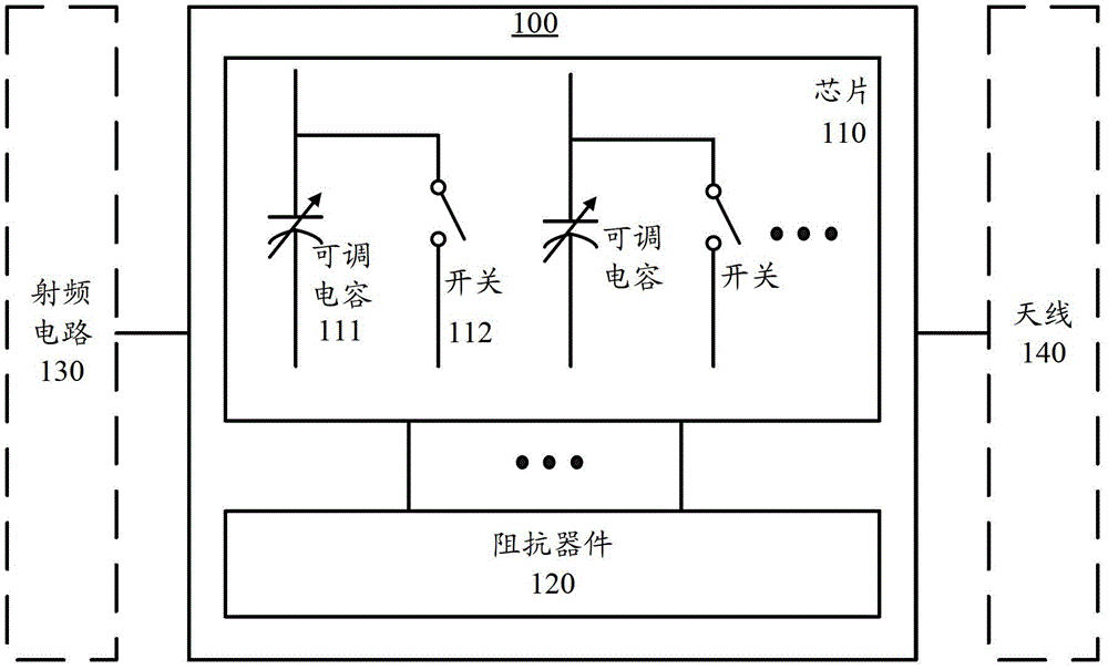
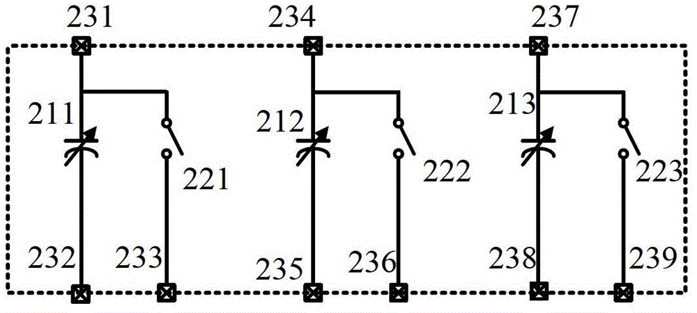
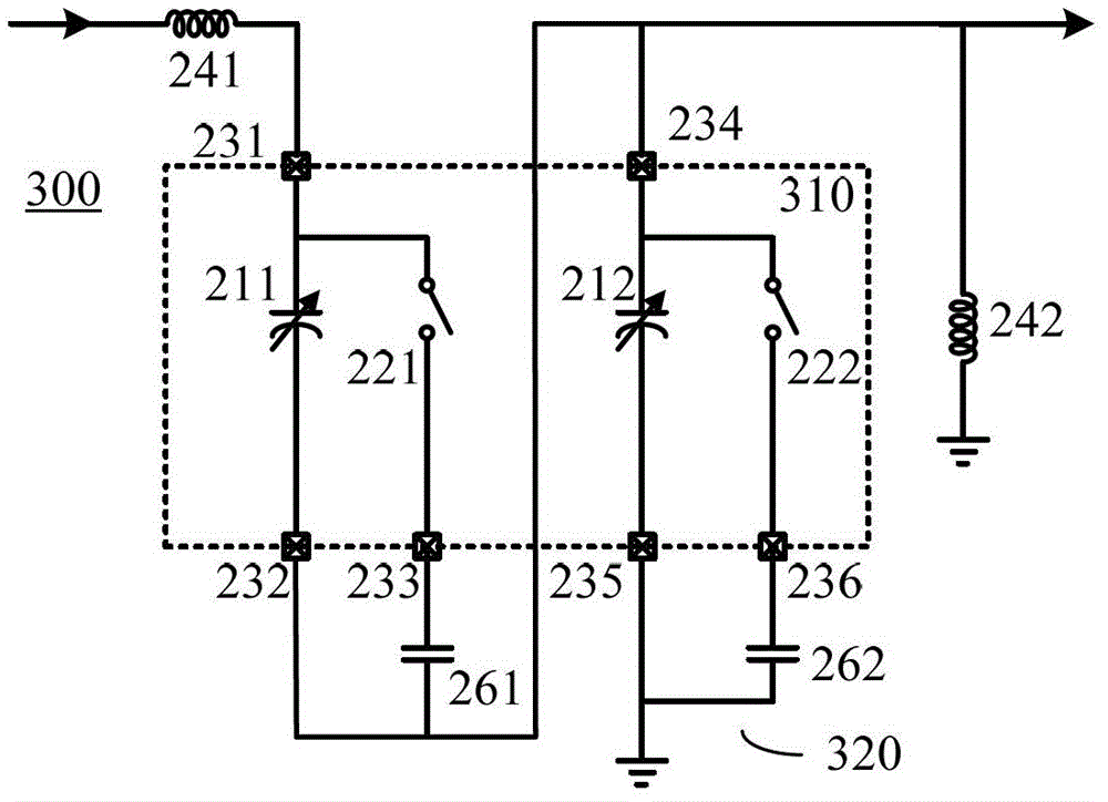
[0049] The technical solutions in the embodiments of the present invention will be clearly and completely described below with reference to the accompanying drawings in the embodiments of the present invention. Obviously, the described embodiments are part of the embodiments of the present invention, but not all of the embodiments. Based on the embodiments of the present invention, all other embodiments obtained by those of ordinary skill in the art without creative efforts shall fall within the protection scope of the present invention.

[0050] It should be understood that the technical solutions of the present invention can be applied to various communication systems, such as: GSM (Global System of Mobile communication, global mobile communication) system, CDMA (Code Division Multiple Access, code division multiple access) system, CDMA2000 system, WCDMA Wideband Code Division Multiple Access (Wideband Code Division Multiple Access) system, GPRS (General Packet Radio Service,...


PUM


Abstract

The invention provides an antenna impedance matching device, a semi-conductor chip and an antenna impedance matching method. The device comprises the semi-conductor chip and at least one impedance device, wherein the semi-conductor chip comprises a plurality of adjustable capacitors and a plurality of switches; the impedance device is located outside the semi-conductor chip; the semi-conductor chip is coupled with the impedance device through a plurality of terminals and coupled with the input end and the output end of the antenna impedance matching device; the input end and the output end of the antenna impedance matching device are respectively coupled with a radio frequency circuit and an antenna; the switches are used for switching the connection between the adjustable capacitors and the impedance device under the control of a control signal; the values of the adjustable capacitors are adjusted by adjustment signals so as to tune the impedance matching of the antenna. The embodiment of the invention can improve the frequency coverage of antenna impedance tuning so as to flexibly tune impedance matching as required.

Description

technical field [0001] The present invention relates to the field of communication technologies, and in particular, to an antenna impedance matching device, a semiconductor chip and a method. Background technique [0002] The antenna impedance of the user equipment is easily affected by the external environment. For example, common actions such as holding the user equipment, bringing the user equipment close to the head, or putting the user equipment in a pocket may cause the antenna impedance to change significantly. For an RF transceiver system, when the impedance mismatch occurs at the antenna port, the communication performance will be deteriorated, for example, the efficiency of the power amplifier will be reduced, the transmit power will be reduced, the power consumption of the whole machine will be increased, the noise figure of the receiver will be deteriorated, and the sensitivity will be reduced. In addition, with the deployment of the LTE system, the frequency ran...

Claims


Application Information

Patent Timeline
Patent Type & Authority Applications(China)
IPC IPC(8): H01Q23/00H01Q1/50
CPCH01Q1/242H03H7/38H03H2007/386H01Q1/50H03H7/383
Inventor 李伟男刘涛梁建
Owner HUAWEI TECH CO LTD
Why Eureka
Try Eureka