

Method of silicon substrate III-V group nanowire area selection transverse epitaxial growth
A lateral epitaxial growth, III-V technology, applied in nanotechnology, electrical components, semiconductor/solid-state device manufacturing, etc., can solve problems affecting the electrical properties of nanowires, growth equipment cavity pollution, etc., and achieve dislocation-free growth. , low surface free energy, low cost effect
- Summary
- Abstract
- Description
- Claims
- Application Information
AI Technical Summary
Problems solved by technology
Method used
Image

Examples
Embodiment Construction
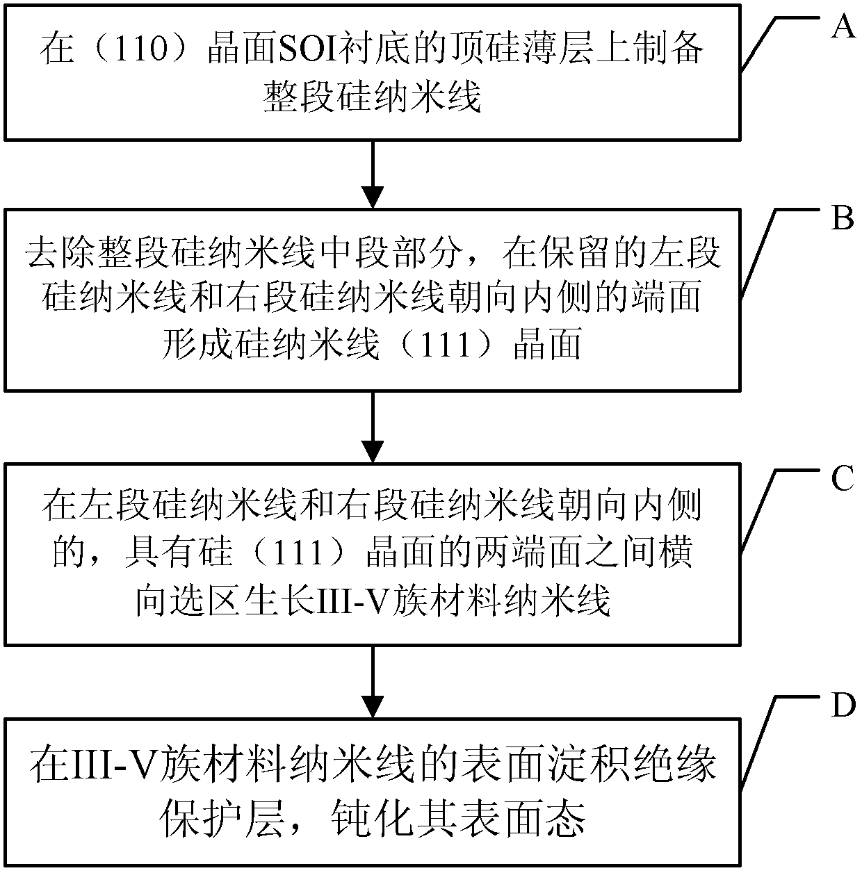
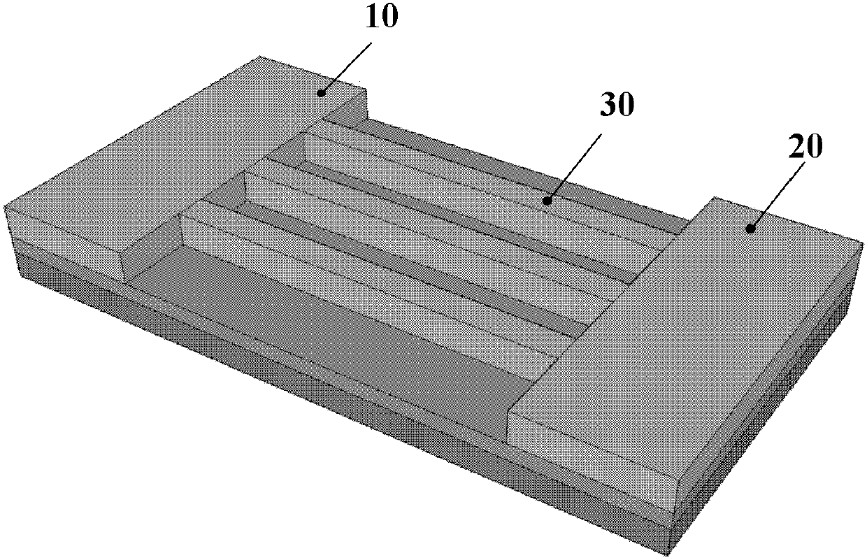
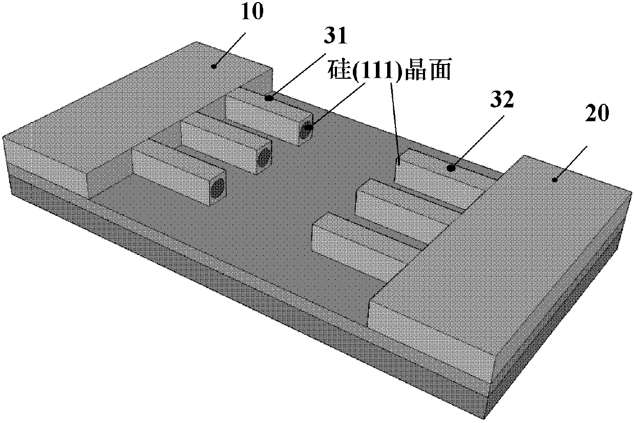
[0024] In order to make the object, technical solution and advantages of the present invention clearer, the present invention will be described in further detail below in conjunction with specific embodiments and with reference to the accompanying drawings.
[0025] It should be noted that, in the drawings or descriptions of the specification, similar or identical parts all use the same figure numbers. Implementations not shown or described in the accompanying drawings are forms known to those of ordinary skill in the art. Additionally, while illustrations of parameters including particular values may be provided herein, it should be understood that the parameters need not be exactly equal to the corresponding values, but rather may approximate the corresponding values within acceptable error margins or design constraints. In addition, the directional terms mentioned in the following embodiments, such as "upper", "lower", "front", "rear", "left", "right", etc., are only re...
PUM
 Abstract
Description
Claims
Application Information