Supercharge Your Innovation With Domain-Expert AI Agents!

Method for detecting alignment degree between polycrystalline silicon grid and contact hole

A technology of polysilicon gate and contact hole, which is applied in the field of detecting the alignment of polysilicon gate and contact hole, can solve the problems affecting the detection accuracy and errors, and achieve the effect of online manufacturing and yield improvement guarantee

Inactive Publication Date: 2013-10-09
SHANGHAI HUALI MICROELECTRONICS CORP
View PDF4 Cites 12 Cited by
  • Summary
  • Abstract
  • Description
  • Claims
  • Application Information

AI Technical Summary

Problems solved by technology

This patent uses an optical method to detect the contact hole. Due to the use of optical means, there will inevitably be errors when the critical size of the detected structure is small, thereby affecting the accuracy of the detection; in addition The patent does not involve detection methods for contact holes and polysilicon alignment

Method used


Image

  • Method for detecting alignment degree between polycrystalline silicon grid and contact hole
  • Method for detecting alignment degree between polycrystalline silicon grid and contact hole

Examples


preparation example Construction

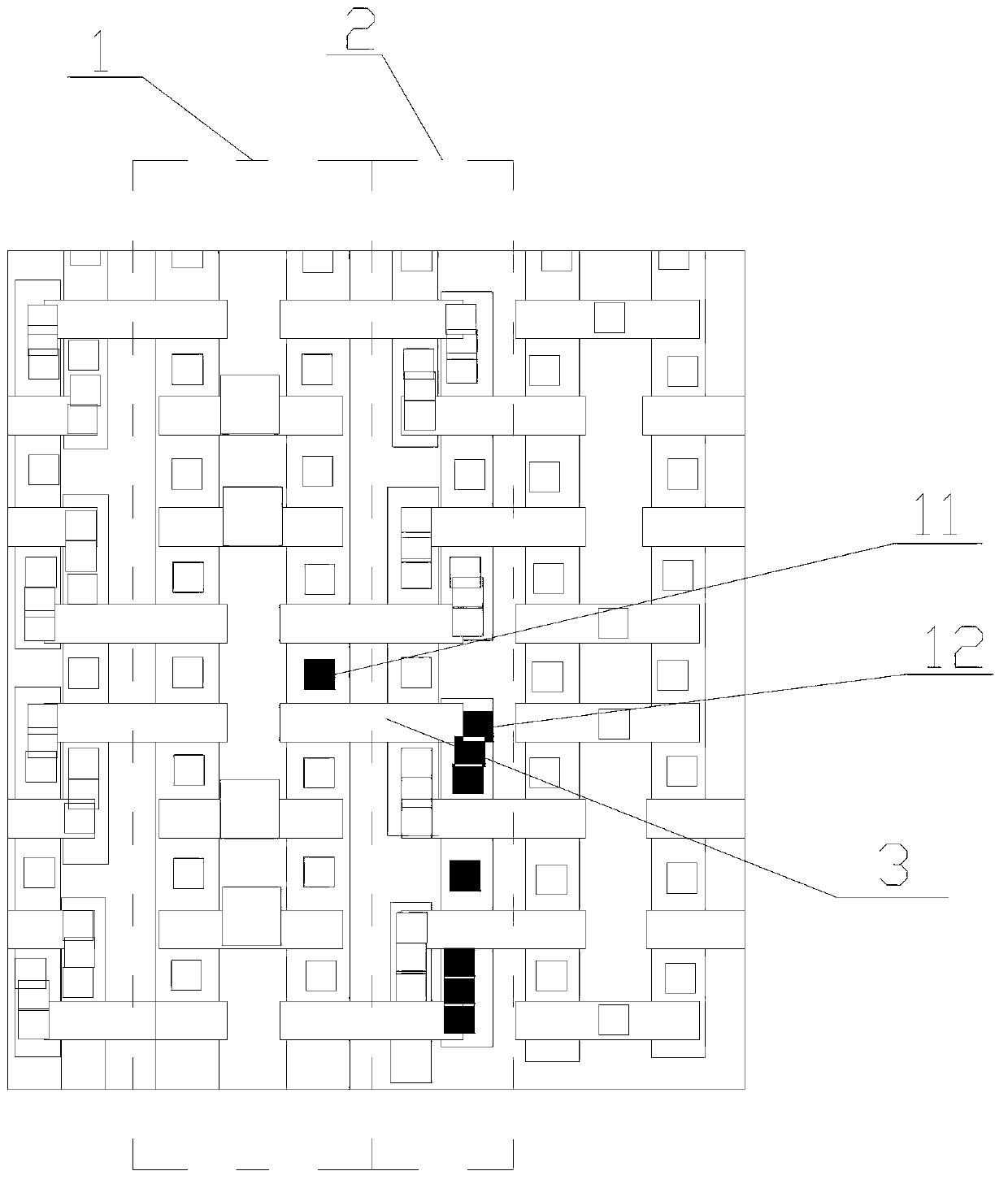
[0036] The preparation process of the test wafer is as follows: a wafer is followed by the normal product wafer tape-out process to the well implantation ion process step, in which the well implantation ion process of the product wafer is slightly changed, specifically, skip Go through the process steps of P-well ion implantation, and change the N-well ion implantation process to non-photoresist ion implantation, so that all the well regions on the substrate of the detection wafer become N-type; then, follow the conventional tape-out process , from the detection wafer tape-out to the active region ion implantation process step, in which the active area ion implantation process of the product wafer is slightly changed, specifically, the ion implantation process step of the N-type active area is skipped , and change the P-type active area ion implantation process to ion implantation without photoresist, so that all the active areas of the detection wafer are P-type active areas, ...


PUM


Abstract

The invention relates to a method for detecting the alignment degree between a polycrystalline silicon grid and a contact hole. The method comprises the steps of providing a detection wafer; carrying out well region ion implantation on the detection wafer by means of a first type of ions so as to form a well region of the same type in the detection wafer; carrying out active region ion implantation on the detection wafer by means of a second type of ions so as to form an active region of the same type in the detection wafer; carrying out contact hole flattening on the detection wafer after manufacturing a grid structure and the contact hole on the detection wafer with the well region and the active region, and continuing to detect the detection wafer to determine the position of the electricity leakage contact hole; detecting the alignment degree between the polycrystalline silicon grid and the contact hole according to the position of the electricity leakage contact hole. The first type of ions and the second type of ions are opposite in terms of type.

Description

technical field [0001] The invention relates to a detection method in the manufacturing process of a semiconductor chip, in particular to a method for detection of the alignment degree of a polysilicon gate and a contact hole. Background technique [0002] With the development of integrated circuit technology, the critical dimensions of integrated circuit devices are being reduced proportionally, which brings with it the continuous improvement of process requirements. Therefore, in the manufacturing process of existing tiny devices, the process accuracy The requirements are getting higher and higher, especially the accuracy of the connection between different structures is particularly important. [0003] Since today's integrated circuit technology requires the critical dimension to be smaller and smaller, the accuracy of the connection between the contact hole and the device structure becomes more and more important when the critical dimension is very small, especially when...

Claims


Application Information

Patent Timeline
Patent Type & Authority Applications(China)
IPC IPC(8): H01L21/66
Inventor 范荣伟倪棋梁陈宏璘龙吟
Owner SHANGHAI HUALI MICROELECTRONICS CORP
Features
  • R&D
  • Intellectual Property
  • Life Sciences
  • Materials
  • Tech Scout
  • Unparalleled Data Quality
  • Higher Quality Content
  • 60% Fewer Hallucinations
Learn More