Touch drive circuit, optical embedded touch screen and display device

A touch drive circuit and driver technology, which is applied in electrical digital data processing, instruments, calculations, etc., can solve problems such as affecting the accuracy of touch screen touch signal detection, increasing touch screen wiring area, and signal crosstalk.

Inactive Publication Date: 2013-10-16
BOE TECH GRP CO LTD +1
View PDF7 Cites 25 Cited by
  • Summary
  • Abstract
  • Description
  • Claims
  • Application Information

AI Technical Summary

Problems solved by technology

[0004] The main disadvantage of the above-mentioned existing optical embedded touch screen drive circuit is: if the touch signal reading ends of the drive circuits at all levels are connected to the same touch signal read line, the touch signals of the drive circuits at different levels will The signals output by the signal reading end will crosstalk with each other, which will affect the accuracy of the touch signal detection of the touch screen; Medium wiring area increases

Method used


Image

  • Touch drive circuit, optical embedded touch screen and display device
  • Touch drive circuit, optical embedded touch screen and display device
  • Touch drive circuit, optical embedded touch screen and display device

Examples


example 1

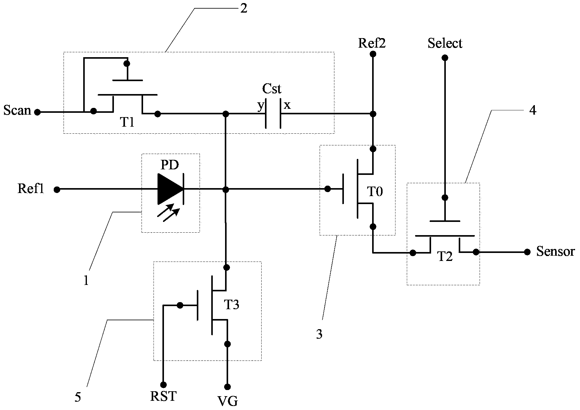
[0054] Such as Figure 2a As shown, the drive transistor T0 , the first switch transistor T1 , the second switch transistor T2 and the third switch transistor T3 are all N-type transistors. Figure 3a for Figure 2a The timing diagram of the circuit, where the voltage of the scanning signal terminal is V Scan , the voltage at the reset control signal terminal is V RST , the voltage at the control signal terminal is V Select , the drain of the driving transistor T0 has a voltage of V when there is a touch A1 , the drain of the drive transistor T0 is V when there is no touch A2 , the voltage of the touch signal reading terminal Sensor is V when there is a touch B1 , the voltage of the touch signal reading terminal Sensor is V when there is no touch B2 .

[0055] Specifically, the working principle of the touch driving circuit is as follows:

[0056] The first stage 1: Scan the voltage V of the signal terminal Scan In high level, reset the voltage V of the control signal...

example 2

[0063] Such as Figure 2b As shown, the driving transistor T0 and the first switch transistor T1 are N-type transistors, and the second switch transistor T2 and the third switch transistor T3 are P-type transistors. Figure 3b for Figure 2b The timing diagram of the circuit, where the voltage of the scanning signal terminal is V Scan , the voltage at the reset control signal terminal is V RST , the voltage at the control signal terminal is V Select , the drain of the driving transistor T0 has a voltage of V when there is a touch A1 , the drain of the drive transistor T0 is V when there is no touch A2 , the voltage of the touch signal reading terminal Sensor is V when there is a touch B1 , the voltage of the touch signal reading terminal Sensor is V when there is no touch B2 .

[0064] Specifically, the working principle of the touch driving circuit is as follows:

[0065] The first stage 1: Scan the voltage V of the signal terminal Scan , Reset control signal termina...

example 3

[0072] Such as Figure 2c As shown, the driving transistor T0, the first switching transistor T1, the second switching transistor T2 and the third switching transistor T3 are all P-type transistors. Figure 3c for Figure 2c The timing diagram of the circuit, where the voltage of the scanning signal terminal is V Scan , the voltage at the reset control signal terminal is V RST , the voltage at the control signal terminal is V Select , the drain of the driving transistor T0 has a voltage of V when there is a touch A1 , the drain of the drive transistor T0 is V when there is no touch A2 , the voltage of the touch signal reading terminal Sensor is V when there is a touch B1 , the voltage of the touch signal reading terminal Sensor is V when there is no touch B2 .

[0073] Specifically, the working principle of the touch driving circuit is as follows:

[0074] The first stage 1: Scan the voltage V of the signal terminal Scan At low level, reset the voltage V of the contro...


PUM


Abstract

The invention discloses a touch drive circuit, an optical embedded touch screen and a display device, wherein the touch drive circuit comprises a light sensitive submodule, a data writing submodule, a drive submodule and a control submodule. Under the control of a scanning signal terminal, the data writing submodule transmits a scanning signal of the scanning signal terminal to the drive submodule; when the drive submodule is controlled to be opened by the scanning signal, the drive submodule outputs a touch sensing signal to the control submodule, and the touch sensing signal is reduced with increasing of light intensity of the light sensitive submodule; and under the control of a control signal terminal, the control submodule inputs the touch sensing signal to a touch signal reading terminal, so that the touch function is realized. Compared with a drive circuit of a conventional optical embedded touch screen, the control submodule is used for controlling the drive submodule to transmit the touch sensing signal to the touch signal reading terminal, and when the touch signal reading terminal of each level of drive circuits is connected with the same touch signal reading wire, signals output by different levels of drive circuits can be prevented from mutual crosstalk.

Description

technical field [0001] The invention relates to the technical field of touch screens, in particular to a touch drive circuit, an optical embedded touch screen and a display device. Background technique [0002] With the rapid development of display technology, touch screen panels (Touch Screen Panels) have gradually spread throughout people's lives. At present, the in-cell touch panel (In Cell Touch Panel) is favored by major panel manufacturers because the touch components are embedded inside the display screen, which can not only reduce the overall thickness of the module, but also greatly reduce the production cost of the touch screen. . Therefore, the driving method of the embedded touch screen has also become a hot spot for people to study the touch screen. [0003] The existing driving circuit of the optical embedded touch screen is a multi-level driving circuit composed of driving circuits of various levels for realizing the touch function. Wherein, the signals of ...

Claims


Application Information

Patent Timeline
Patent Type & Authority Applications(China)
IPC IPC(8): G06F3/042
CPCG06F3/0412G06F3/0416G06F3/042G06F3/0421
Inventor 聂磊森祁小敬周全国
Owner BOE TECH GRP CO LTD
Why Eureka
Try Eureka