Method for handling electroplating lead layout of IC packaging base plate and electroplating lead structure

A technology of electroplating lead wires and packaging substrates, which is applied in the direction of circuits, electrical components, and electrical solid devices, which can solve problems such as signal loss, increase the difficulty of wiring, and interference, so as to ensure the improvement of signal and electrical performance and reduce the wiring area. Effect

Inactive Publication Date: 2005-01-19
美龙翔微电子科技(深圳)有限公司
View PDF0 Cites 9 Cited by
  • Summary
  • Abstract
  • Description
  • Claims
  • Application Information

AI Technical Summary

Problems solved by technology

This kind of remaining electroplating lead causes signal loss and interference to the high-speed signal line on the high-frequency and high-speed packaging substrate, affecting the integrity of the signal
At the same time, it increases the difficulty of wiring, and even in the case of very high-density wiring, it is impossible to realize the arrangement of plating leads

Method used


Image

  • Method for handling electroplating lead layout of IC packaging base plate and electroplating lead structure
  • Method for handling electroplating lead layout of IC packaging base plate and electroplating lead structure
  • Method for handling electroplating lead layout of IC packaging base plate and electroplating lead structure

Examples


Embodiment Construction

[0029] Further description below in conjunction with accompanying drawings.

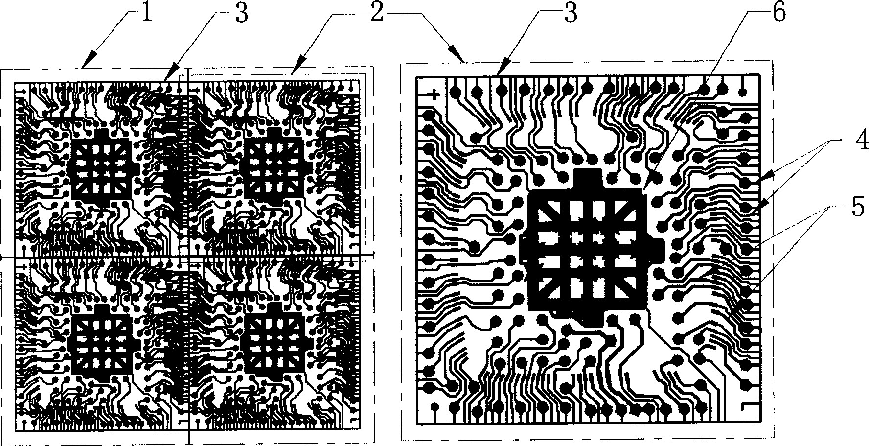
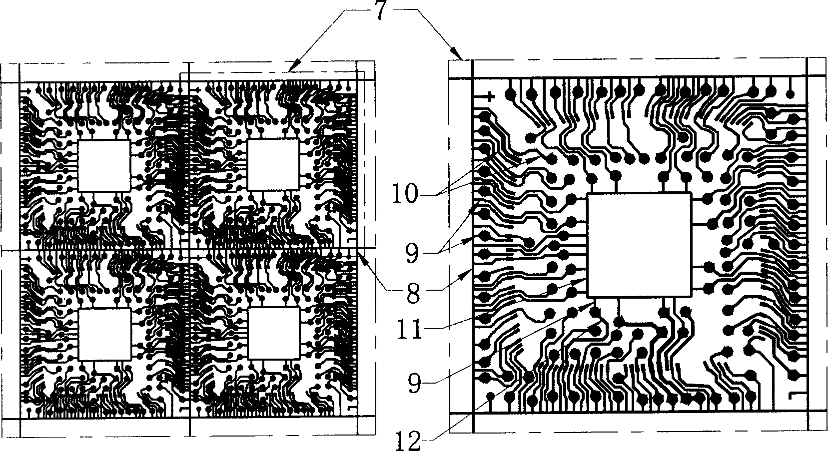
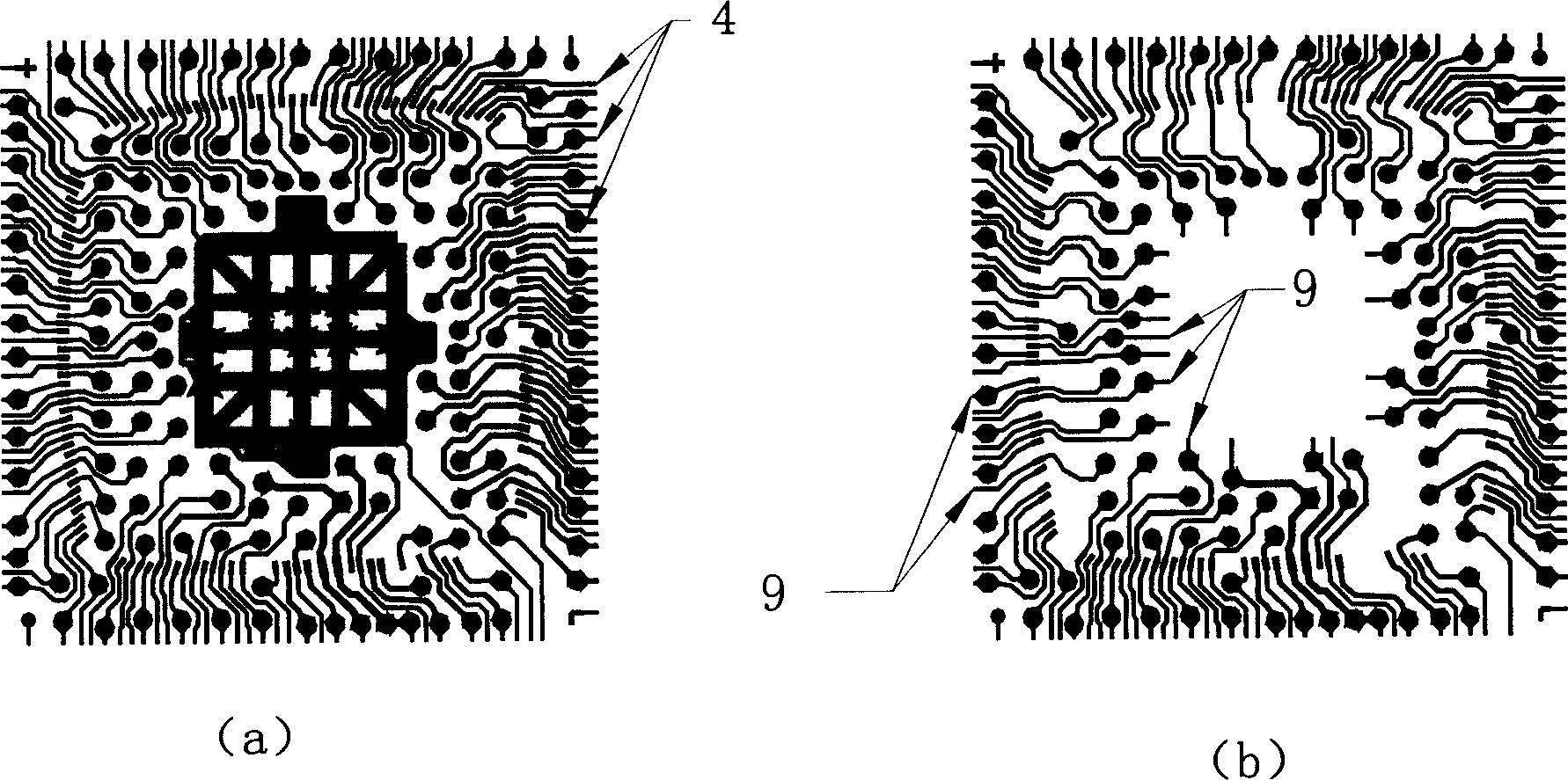
[0030] Figure 4 It is a schematic diagram of the circuit structure of the packaging substrate unit applying the present invention, Figure 5 yes Figure 4 A partial enlarged view of the electroplating lead in the packaging substrate unit, a partial enlarged view of the connection between the electroplating lead and the metallized micro-via hole, and a cross-sectional view of the metallized via hole. The electroplating lead structure in the schematic integrated circuit package substrate unit includes the IC package substrate unit (13), and the electroplating lead (15) is set between the wire patterns (14) in the package substrate unit (13), and the wire pattern (14) Each wire is connected to the electroplating lead (15) nearby, and the electroplating lead (15) passes through the metallized micro-via hole (16) and passes through the insulating medium layer (17) to communicate with the metal power su...


PUM


Abstract

The invention relates to a processing method of plating wire distribution of IC packing substrate, including: a. arranging plating wires between wire patterns in packing substrate units to make all the wires of the wire patterns connect mutually by plating wires, where the plating wires or wire patterns connect with metal power supply layers in packing substrates; b. making plating treatment on the packing substrates and eliminating the plating wires by chemically etching process. The invention public plating wires between wire patterns in the packing substrates units, where the plating public wires are thinner than the wire patterns and narrower than the narrowest wire pattern, and eliminates the public wires by etching process, can make the shape change of the wire patterns minimum by controlling etching process conditions, thus beneficial to the improvement of electric performance of the substrate, assuring the integrity of signals and able to reduce wiring area, especially applied to make high-frequency high-speed IC packing substrates.

Description

technical field [0001] The invention relates to a semiconductor circuit packaging substrate manufacturing technology, in particular to a method for laying out electroplating lead wires on an integrated circuit packaging substrate, and an electroplating lead structure on the substrate. Background technique [0002] With the miniaturization and thinning of the development of integrated circuits, the requirements for integrated circuit packaging are also increasing, and the requirements for packaging substrates are more light, thin, short, and small to ensure good electrical performance. In order to meet the above requirements, a high wiring density is necessary, and the structure of the plating leads on the outer layer of the packaging substrate has a great influence on the wiring density and the electrical performance after packaging. [0003] At present, the following two methods are usually used for the layout of the common connection lines for the plating of printed semico...

Claims


Application Information

Patent Timeline
Patent Type & Authority Applications(China)
IPC IPC(8): H01L21/48H01L21/60H01L23/12H01L23/495
CPCH01L2924/0002
Inventor 尤宁圻朱惠贤陈金富
Owner 美龙翔微电子科技(深圳)有限公司
Why Eureka
Try Eureka