

Active clamping high gain boost converter using coupling inductor
A coupled inductor and high-gain technology, which is applied in the field of active clamp high-gain boost converters, can solve the problems of high voltage spikes generated by its own leakage inductance, large voltage stress of power switch tubes, etc., to solve high voltage spikes, Reduced voltage stress and high output gain
- Summary
- Abstract
- Description
- Claims
- Application Information
AI Technical Summary
Problems solved by technology
Method used
Image

Examples
Embodiment 1
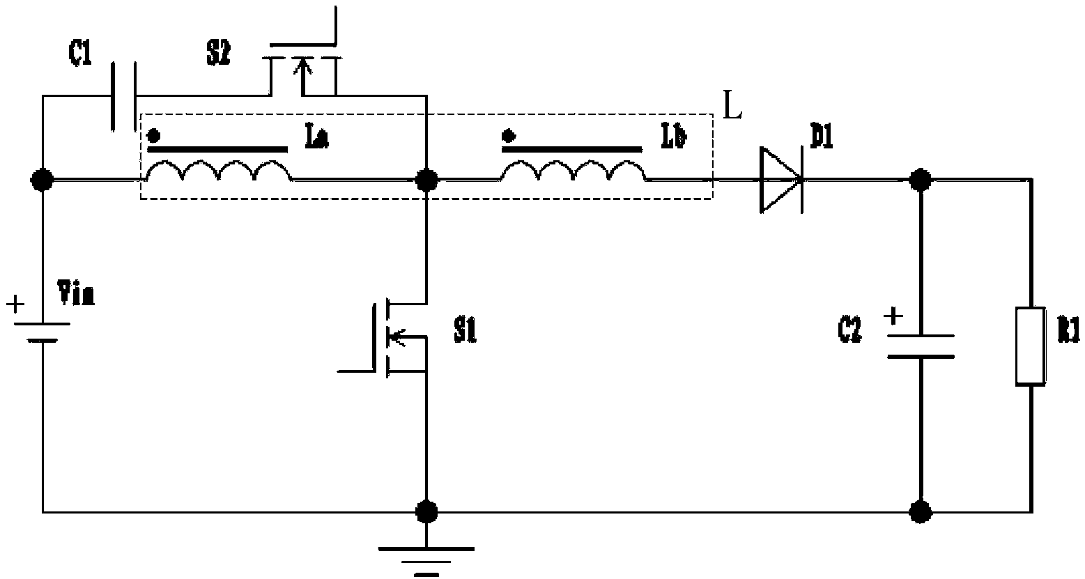
[0020] Such as figure 1 As shown, the active-clamp high-gain boost converter using coupled inductors includes a power switch S1, a clamp switch S2, a freewheeling diode D1, a clamp capacitor C1, and an output filter capacitor C2. A coupled inductor L. The coupled inductor L has two windings La, Lb, one end of the first winding La is connected to the positive end of the power supply Vin, the other end of the first winding La is connected to the drain of the power switch S1 and the source of the clamping switch S2 and the second One end of the second winding Lb is connected, the other end of the second winding Lb is connected to the anode of the freewheeling diode D1, the cathode of the freewheeling diode D1 is connected to the positive end of the output filter capacitor C2 and one end of the load R1, and the source of the power switch S1 The pole is connected to the negative end of the output filter capacitor C2 and the other end of the load resistor R1 is connected to the neg...
Embodiment 2
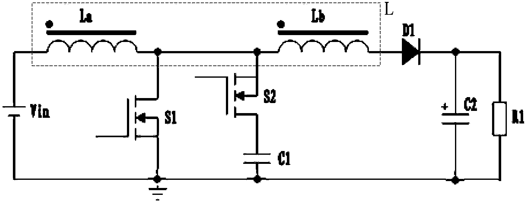
[0023] Such as figure 2 As shown, the difference from Embodiment 1 is that the other end of the clamping capacitor C1 connected to the drain of the clamping switch S2 is connected to the negative terminal of the power supply Vin.
Embodiment 3
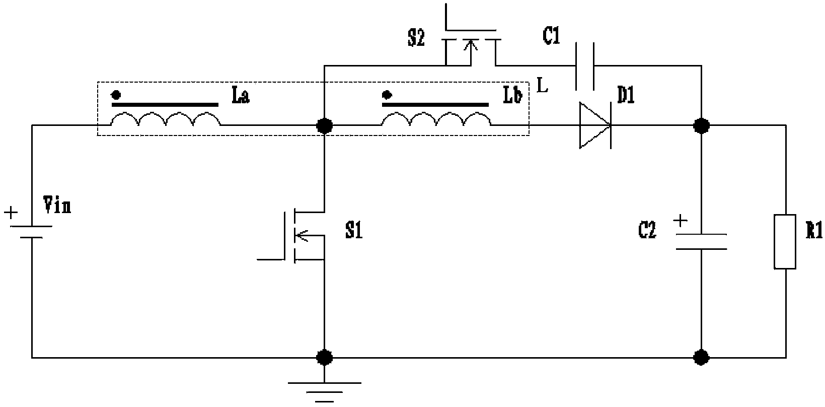
[0025] Such as image 3 As shown, the difference from Embodiment 1 is that the other end of the clamping capacitor C1 connected to the drain of the clamping switch S2 is connected to the cathode of the freewheeling diode D1.
[0026] When the converter is working, in one switching cycle, the power switch tube S1 is first turned on, the first winding La of the coupling inductor charges and stores energy, and the positive voltage is induced on the second winding Lb of the coupling inductor, the freewheeling diode D1 is reversely cut off, and the load R1 Energy is provided by the output filter capacitor C2 to maintain the output voltage. When the power switch S1 is turned off, the clamp switch S2 is turned on, and the clamp capacitor C1 absorbs leakage inductance energy. At the same time, part of the energy in the first winding La of the coupled inductor is transferred to the second winding Lb of the coupled inductor when the power switch tube S1 is turned off, and then La, Lb, ...
PUM
 Abstract
Description
Claims
Application Information