Interference exposure system and exposure method thereof

A technology of interference exposure and exposure system, which is used in microlithography exposure equipment, photolithography process exposure devices, etc., and can solve the problems that the resolution is not as good as that of positive photoresist and the high resolution limitation of interference lithography.

Active Publication Date: 2013-10-30
SHANGHAI MICRO ELECTRONICS EQUIP (GRP) CO LTD
View PDF10 Cites 9 Cited by
  • Summary
  • Abstract
  • Description
  • Claims
  • Application Information

AI Technical Summary

Problems solved by technology

[0008] For some application scenarios, such as patterned sapphire substrate PSS, the general process needs to form dense column patterns on the positive photoresist, and the resolution of the negative photoresist is not as good as that of the positive photoresist. High resolution is a limitation

Method used


Image

  • Interference exposure system and exposure method thereof
  • Interference exposure system and exposure method thereof
  • Interference exposure system and exposure method thereof

Examples


no. 1 example

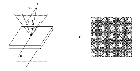
[0059] refer to Figure 4 As shown, the interference exposure system includes a beam splitter 1 , two shutters 21 , 22 , two mirrors 31 , 32 , a glue-coated base 4 , a rotating mechanism 5 and a phase compensator 6 . The incident light 10 passes through the beam splitting device 1 and is split into two beams of light with equal intensity and same polarization state, which are spatially symmetrical, namely a first beam 101 and a second beam 102 . The first light beam 101 and the second light beam 102 are respectively incident on the surface of the glue-coated substrate 4 at the same incident angle after passing through the mirrors 31 and 32 . The two shutters 21 and 22 are respectively arranged in the interference arm where the first light beam 101 and the second light beam 102 are located, and the phase compensator 6 is arranged in the first interference arm where the first light beam 101 is located. The phase compensator 6 can be a wave plate or a liquid crystal phase retarder...

no. 2 example

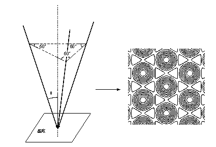
[0063] refer to Figure 9 As shown, the interference exposure system of this embodiment includes a beam splitter 1 , three shutters 21 , 22 , 23 , three mirrors 31 , 32 , 33 , a glue-coated substrate 4 and a phase compensator 6 . This embodiment can also realize the function of forming dense holes and dense column patterns distributed in regular hexagons on the positive photoresist.

[0064] The incident light 20 can be collimated monochromatic coherent light, generally a laser with a wavelength from deep ultraviolet to about 450nm; the incident light passes through the beam splitter 1, is divided into equal intensity and same polarization state, and is projected onto the substrate at a spatial angle 3 beams of light at 120 degrees, namely the first beam 201 , the second beam 202 and the third beam 203 . The three beams of light respectively pass through a reflector 31, 32, 33, are incident at the same incident angle and converge on the surface of the glue-coated substrate. ...

no. 3 example

[0069] This embodiment can realize the formation of regular quadrilateral dense hole and dense column patterns on the positive photoresist. The interference exposure system includes a beam splitter 1 , phase compensators 61 , 62 , four mirrors 31 , 32 , 33 , 34 and a glue-coated substrate 4 . Compared with Embodiment 1, this embodiment omits the rotating mechanism.

[0070] The incident light 30 passes through the beam splitting device 1 and is divided into four beams of equal intensity and same polarization state, which are mapped to the substrate and form an angle of 90 degrees with each other, namely the first beam 301, the second beam 302, the third beam 303 and The fourth light beam 304 . After the four beams of light pass through the reflectors 31, 32, 33, and 34 respectively, they are incident and converged on the surface of the glue-coated substrate 4 with the same incident angle, wherein the first beam 301 and the second beam 302, the third beam 303 and the fourth be...


PUM


Abstract

The invention discloses an interference exposure system which is used for exposing a substrate coated with photoresist. According to the system, incident light is divided into at least two light beams through a beam-splitting device, and at least two interference arms are correspondingly formed; each interference arm is provided with a shutter for controlling whether the interference arm is involved in exposure and the exposure time; at least one interference arm is provided with a phase compensator used for changing the beam phase of the interference arm. The interference exposure method comprises the following steps of: providing a substrate, and coating photoresist on the surface of the substrate; providing incident light, dividing the incident light into two light beams, and correspondingly forming two interference arms; adjusting the beam phase of one interference arm in the two interference arms, so that the beam phase of the interference arm is changed by 180 degrees*N, and N is an integer; performing repeated exposure on the photoresist on the substrate by utilizing the two interference arms, rotating the substrate, and forming multiple groups of interference patterns of which interference fringes are superposed on the photoresist on the substrate. The interference exposure system has the advantages that holes and columnar patterns can be flexibly formed on the positive and negative photoresists.

Description

[0001] technical field [0002] The invention relates to the field of photolithographic exposure, in particular to interference exposure technology. Background technique [0003] Interference lithography uses the interference and diffraction characteristics of light to modulate the light intensity distribution in the interference field through a specific beam combination method, and records it with a photosensitive material to generate a photolithographic pattern. [0004] Interference lithography has the advantage of high resolution, that is, it can reach 1 / 4 of the exposure wavelength relatively easily, and it also has the advantage of large depth of focus, that is, it is close to the coherent wavelength of the light source. Therefore, interference lithography can be used for periodic patterning of tens of nanometers to several microns in size. [0005] U.S. Patent US6285817 proposes a multi-beam interference lithography technology scheme based on spherical waves, whic...

Claims


Application Information

Patent Timeline
Patent Type & Authority Applications(China)
IPC IPC(8): G03F7/20
Inventor 许琦欣何帅王帆
Owner SHANGHAI MICRO ELECTRONICS EQUIP (GRP) CO LTD
Why Eureka
Try Eureka