Schottky semiconductor device with grooves and preparation method thereof

A semiconductor and Schottky potential technology, applied in semiconductor/solid-state device manufacturing, semiconductor devices, electrical components, etc., can solve problems such as low forward turn-on voltage, fast turn-on and turn-off speed, and influence on reverse breakdown characteristics of devices

Active Publication Date: 2013-10-30
北海惠科半导体科技有限公司
View PDF4 Cites 2 Cited by
  • Summary
  • Abstract
  • Description
  • Claims
  • Application Information

AI Technical Summary

Problems solved by technology

[0002] Power semiconductor devices are widely used in power management and power applications, especially semiconductor devices involving Schottky junctions have become an important trend in device development. Schottky devices have the advantages of low forward turn-on voltage and fast turn-on and turn-off speed. At the same time, Schottky devices also have the disadvantages of large reverse leakage current and cannot be used in high-voltage environments.
[0003] Schottky diodes can be manufactured through a variety of different layout techniques, the most commonly used is planar layout, the traditional planar Schottky diode has a sudden electric field distribution curve in the drift region, which affects the reverse breakdown characteristics of the device, while the traditional The planar Schottky diode has a high on-resistance

Method used


Image

  • Schottky semiconductor device with grooves and preparation method thereof
  • Schottky semiconductor device with grooves and preparation method thereof

Examples


Embodiment 1

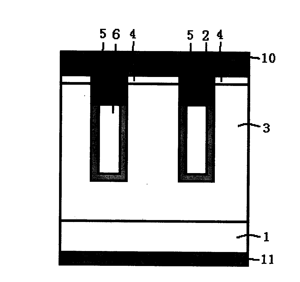
[0021] figure 1 It is a cross-sectional view of a trench Schottky semiconductor device of the present invention, combined below figure 1 The semiconductor device of the present invention will be described in detail.

[0022] A Schottky semiconductor device with a trench, comprising: a substrate layer 1, which is an N-conductive type semiconductor silicon material, and the doping concentration of phosphorus atoms is 1E19 / CM 3 , on the lower surface of the substrate layer 1, the electrodes are drawn out through the lower surface metal layer 11; the first conductive semiconductor material 3, located on the substrate layer 1, is a semiconductor silicon material of N conductivity type, and the doping concentration of phosphorus atoms is 1E15 / CM 3 ; The second conductive semiconductor material 4, located on the first conductive semiconductor material 3, is a semiconductor silicon material of P conductivity type, and the doping concentration of boron atoms is 1E17 / CM 3 ; Schottky b...

Embodiment 2

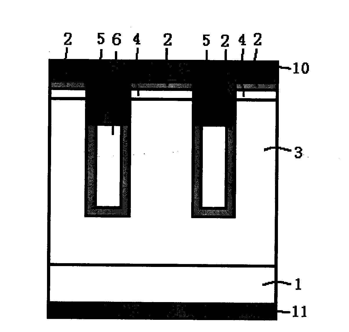
[0033] figure 1 It is the sectional view of the second Schottky semiconductor device with trenches of the present invention, combined below figure 2 The semiconductor device of the present invention will be described in detail.

[0034] A Schottky semiconductor device with a trench, comprising: a substrate layer 1, which is an N-conductive type semiconductor silicon material, and the doping concentration of phosphorus atoms is 1E19 / CM 3 , on the lower surface of the substrate layer 1, the electrodes are drawn out through the lower surface metal layer 11; the first conductive semiconductor material 3, located on the substrate layer 1, is a semiconductor silicon material of N conductivity type, and the doping concentration of phosphorus atoms is 1E15 / CM 3 ; The second conductive semiconductor material 4, located on the first conductive semiconductor material 3, is a semiconductor silicon material of P conductivity type, and the doping concentration of boron atoms is 1E17 / CM 3...


PUM


Abstract

The invention discloses a Schottky semiconductor device with grooves. The Schottky semiconductor device with the grooves comprises an MOS structure, a PN junction and a Schottky barrier junction. The electric field distribution of reverse bias voltage is changed through the MOS structure, and therefore the forward-direction conductive character of a component is improved. The bearing capacity of transient high voltage of the component is improved through the PN junction. When the semiconductor device is under the forward-direction small electric current density state, the PN junction is not opened, and therefore minority carrier injection of the component is reduced, and the reverse recovery character of the component is improved. The invention provides a preparation method of the Schottky semiconductor device with the grooves.

Description

technical field [0001] The invention relates to a Schottky semiconductor device with grooves, and also relates to a preparation method of the Schottky semiconductor device with grooves. The semiconductor device of the present invention is a basic structure for manufacturing power rectifying devices. Background technique [0002] Power semiconductor devices are widely used in power management and power applications, especially semiconductor devices involving Schottky junctions have become an important trend in device development. Schottky devices have the advantages of low forward turn-on voltage and fast turn-on and turn-off speed. At the same time, Schottky devices also have disadvantages such as large reverse leakage current and cannot be used in high-voltage environments. [0003] Schottky diodes can be manufactured through a variety of different layout techniques, the most commonly used is planar layout, the traditional planar Schottky diode has a sudden electric field ...

Claims


Application Information

Patent Timeline
Patent Type & Authority Applications(China)
IPC IPC(8): H01L29/872H01L21/329
Inventor 朱江
Owner 北海惠科半导体科技有限公司
Why Eureka
Try Eureka