A trench Schottky semiconductor device with multiple insulating layer isolation and its preparation method

A semiconductor and insulating layer technology, which is applied in the field of trench Schottky semiconductor devices, can solve the problems of multiple times, high on-resistance and reverse leakage current characteristics, so as to increase the doping concentration, reduce the forward conduction resistance, Effect of Improving Reverse Voltage Blocking Characteristics

Active Publication Date: 2016-08-03
SEMICON MFG ELECTRONICS (SHAOXING) CORP
View PDF4 Cites 0 Cited by
  • Summary
  • Abstract
  • Description
  • Claims
  • Application Information

AI Technical Summary

Problems solved by technology

The manufacturing process of the traditional trench Schottky diode requires more masks and manufacturing steps, and the traditional trench Schottky diode has high on-resistance and reverse leakage current characteristics

Method used


Image

  • A trench Schottky semiconductor device with multiple insulating layer isolation and its preparation method
  • A trench Schottky semiconductor device with multiple insulating layer isolation and its preparation method
  • A trench Schottky semiconductor device with multiple insulating layer isolation and its preparation method

Examples


Embodiment 1

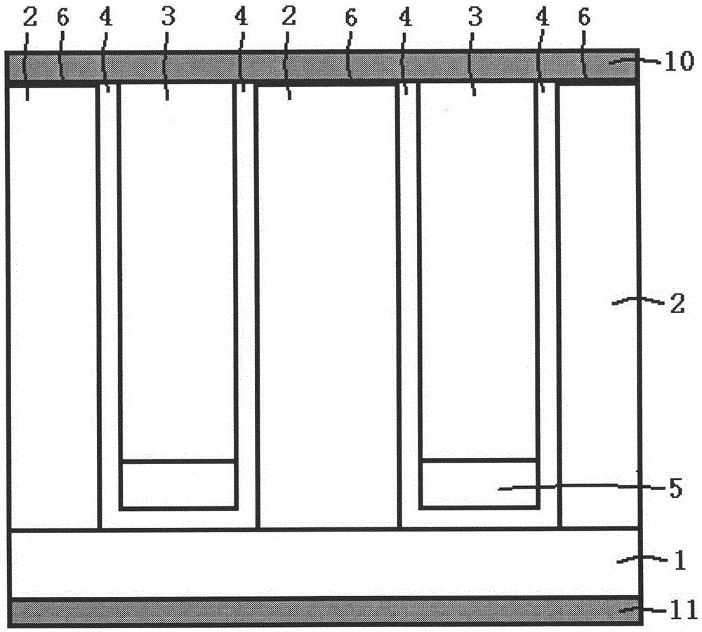
[0035] figure 1 It is a trench Schottky semiconductor device with a variety of insulating layer isolations of the present invention, and the following combination figure 1 The semiconductor device of the present invention will be described in detail.

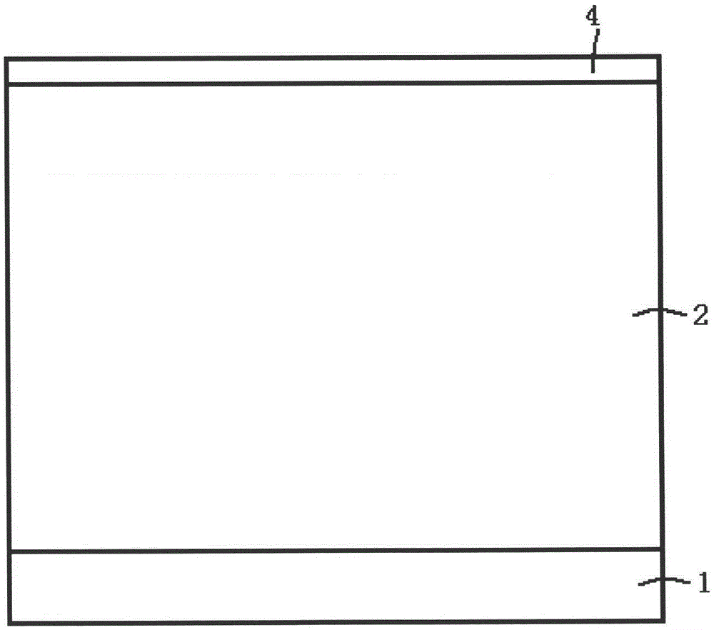
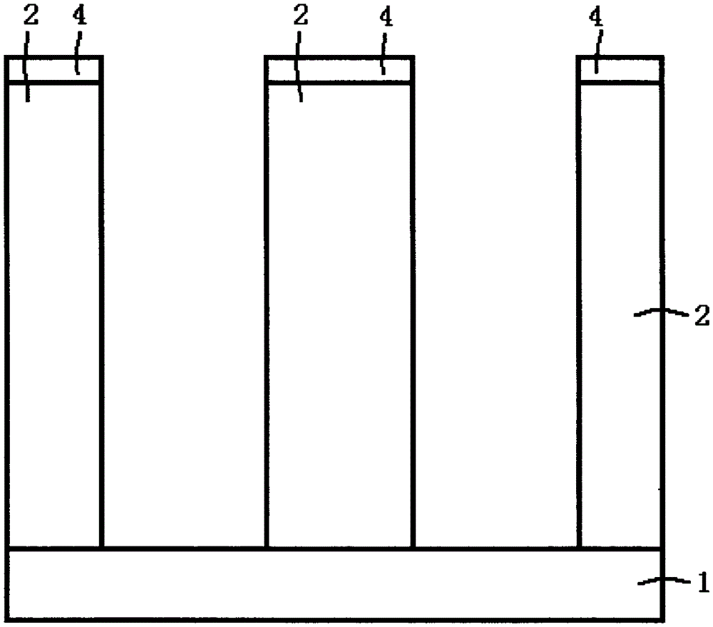
[0036] A trench Schottky semiconductor device with multiple insulating layers isolation, including: a substrate layer 1, which is a semiconductor silicon material of N conductivity type, and the doping concentration of phosphorus atoms is 1E19 / CM 3 , On the lower surface of the substrate layer 1, the electrode is drawn through the lower surface metal layer 11; the N-type semiconductor silicon material 2, located on the substrate layer 1, is a semiconductor silicon material of N conductivity type, and the doping concentration of phosphorus atoms is 1E16 / CM 3 ; P-type semiconductor polysilicon material 3, located on the upper part of the substrate layer 1, is a semiconductor polysilicon material of P conductivity type, and the doping co...


PUM


Abstract

The invention discloses a trench Schottky semiconductor device with various insulating layer isolation. Through various insulating layer structures, the electric field intensity distribution of drift regions is changed, and inverse voltage blocking properties of apparatuses are improved. The invention further provides a preparation method capable of achieving two-time photolithography processes to manufacture apparatuses.

Description

Technical field [0001] The invention relates to a trench Schottky semiconductor device with a variety of insulating layer isolations, and the invention also relates to a method for preparing a trench Schottky semiconductor device with a variety of insulating layer isolations. Background technique [0002] Power semiconductor devices are widely used in power management and power applications. Especially semiconductor devices involving trench structures have become an important trend in device development. Schottky devices have the advantages of low forward turn-on voltage and fast turn-on and turn-off speed. At the same time, Schottky devices also have the disadvantages of large reverse leakage current and cannot be used in high-voltage environments. [0003] Schottky diodes can be manufactured through a variety of different layout techniques, the most commonly used planar layout. A typical trench layout is shown in BJBaliga's Patent No. 5612567. The traditional trench-type Schott...

Claims


Application Information

Patent Timeline
Patent Type & Authority Patents(China)
IPC IPC(8): H01L29/872H01L29/06H01L21/329
Inventor 朱江盛况
Owner SEMICON MFG ELECTRONICS (SHAOXING) CORP
Why Eureka
Try Eureka