Lift off method
An optical device and epitaxial substrate technology, applied in the lift-off field, can solve the problems of uneven damage to the buffer layer, inability to properly peel off the epitaxial substrate, etc.
- Summary
- Abstract
- Description
- Claims
- Application Information
AI Technical Summary
Problems solved by technology
Method used
Image
Examples
Embodiment Construction
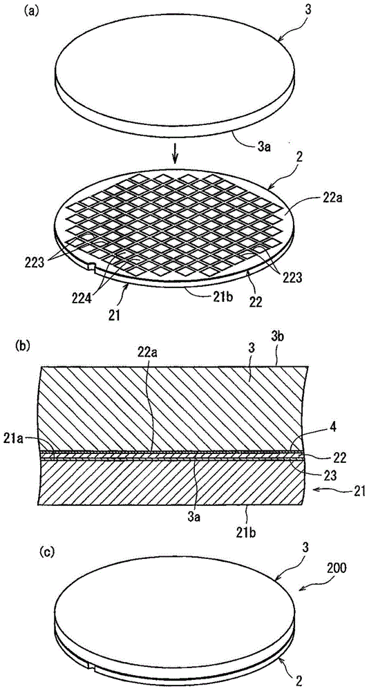
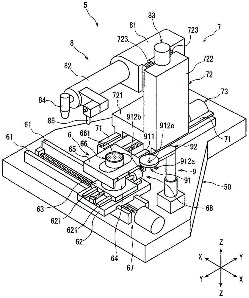
[0049] Hereinafter, preferred embodiments of the lift-off method according to the present invention will be described in detail with reference to the drawings.
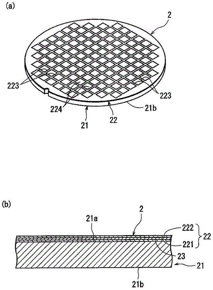
[0050] figure 1 (a) and (b) show a perspective view and an enlarged sectional view of main parts of an optical device wafer on which an optical device layer transferred to a transfer substrate by the lift-off method of the present invention is formed.
[0051] figure 1 In the optical device wafer 2 shown in (a) and (b), an optical device composed of an n-type gallium nitride semiconductor layer 221 and a p-type gallium nitride semiconductor layer 222 is formed on the surface 21a of the epitaxial substrate 21 by the epitaxial growth method. The device layer 22, wherein the epitaxial substrate 21 is composed of a disc-shaped sapphire substrate with a diameter of 50 mm and a thickness of 600 μm. In addition, when the optical device layer 22 composed of the n-type gallium nitride semiconductor layer 221 and the p-type g...
PUM
 Abstract
Description
Claims
Application Information


