Vertical shape measuring device capable of compensating shaft system errors of wafer

A technology of measuring device and compensating shaft, applied in the direction of measuring device, using optical device, instrument, etc., can solve the problems of uneven measuring force, affecting measuring accuracy, uncontrollable, etc., to solve the problem of inaccurate measuring accuracy, improve measuring accuracy, simple structure

Inactive Publication Date: 2013-11-13
KUNSHAN YUNCO PRECISION IND TECH
View PDF7 Cites 14 Cited by
  • Summary
  • Abstract
  • Description
  • Claims
  • Application Information

AI Technical Summary

Problems solved by technology

[0003] Traditional wafer measurement equipment is divided into two types: contact type and non-contact type in terms of measurement methods: traditional contact type measurement equipment has a single function for wafer measurement and cannot measure flatness and thickness on the same equipment. , the measurement force is difficult to control accurately, which affects the measurement accuracy of each point, and even causes the wafer to break during the measurement process due to uneven and uncontrollable measurement force. The non-contact wafer measuring instrument uses laser irradiation for measurement. Due to the different reflective effects of different measurement materials, it is difficult to unify the measurement data of each layer, especially for the measurement of the glass layer and the high-brightness surface after the finished product, the measurement accuracy will be affected by the transparency of the material or the high brightness of the surface, resulting in distortion of the measurement data, making it difficult to be accurate Judging the authenticity of the measurement data, since the X-axis drives the probe to move left and right during the measurement process, the motion error of the axis system will inevitably be introduced into the final measurement result

Method used


Image

  • Vertical shape measuring device capable of compensating shaft system errors of wafer
  • Vertical shape measuring device capable of compensating shaft system errors of wafer
  • Vertical shape measuring device capable of compensating shaft system errors of wafer

Examples


Embodiment Construction

[0016] Embodiments of the present invention are described in detail below, examples of which are shown in the drawings, wherein the same or similar reference numerals designate the same or similar elements or elements having the same or similar functions throughout. The embodiments described below by referring to the figures are exemplary only for explaining the present invention and should not be construed as limiting the present invention.

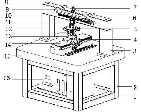
[0017] see Figure 1 to Figure 4 As shown, a vertical wafer shape measuring device capable of compensating shaft system errors includes a steel frame base 2; an electric control cabinet 16, the electric control cabinet 16 is installed inside the steel frame base 2, and the electric control cabinet 16 There is an electric control system; industrial computer 1, the industrial computer 1 is located on the side of the electric control cabinet 16, the inside of the steel frame base 2; a granite platform 15, the platform 15 is located on the ...


PUM


Abstract

A vertical shape measuring device capable of compensating shaft system errors of a wafer, which comprises a steel frame base, a platform, a support seat, a beam, a shaft system, a wafer bearing table, a contact-type length measuring device, and an optical flat, wherein the platform is arranged on the steel frame base; the support seat is arranged on the platform; the beam is arranged on the support seat; the shaft system comprises an X shaft, a Y shaft, a Z shaft, and a rotating shaft, the X shaft is arranged on the beam, the Y shaft is arranged on the platform and is perpendicular to the X shaft mutually, the Z shaft is fixed on an X shaft movable plate and is perpendicular to the motion direction of the X shaft mutually, the motion direction of the Z shaft is perpendicular to the measuring platform, and the rotating shaft is fixed on a Y shaft movable plate; the wafer bearing table is fixed on the rotating shaft; the contact-type length measuring device is fixed on a Z shaft movable plate; the optical flat is fixed on the beam parallel to the motion direction of the X shaft. The shape measuring device has simple structure, high integrated level, and full functions, and provides a solution for the measuring of wafer shape parameters.

Description

technical field [0001] The invention relates to a measuring device, in particular to a vertical wafer shape measuring device capable of compensating shaft error. Background technique [0002] In order to meet the gradually expanding demand for global energy, solar energy is widely used as a green energy source, and as a key component of solar circuit boards, the demand and quality of wafers are constantly increasing. Wafers are generally made of multiple layers of different materials (the first layer polysilicon, the second layer is adhesive, the third layer is glass, and the fourth layer is adhesive tape) is made by lamination process, usually from the first layer to the fourth layer by layer lamination, and each layer is laminated after lamination The degree of lamination and the thickness after lamination need to be closely monitored, and the flatness and thickness of the finished wafer after lamination of all 4 layers also need to be tested. Only products that meet the q...

Claims


Application Information

Patent Timeline
Patent Type & Authority Applications(China)
IPC IPC(8): G01B11/30G01B11/06
Inventor 夏发平
Owner KUNSHAN YUNCO PRECISION IND TECH
Why Eureka
Try Eureka