Photoresist cleaning liquid

A cleaning solution and photoresist technology, applied in the processing of photosensitive materials, etc., can solve the problems of insufficient cleaning ability, wafer pattern and substrate corrosion, etc., and achieve the effect of mild operating temperature and strong removal ability

Inactive Publication Date: 2013-11-13
ANJI MICROELECTRONICS TECH (SHANGHAI) CO LTD
View PDF9 Cites 3 Cited by
  • Summary
  • Abstract
  • Description
  • Claims
  • Application Information

AI Technical Summary

Problems solved by technology

[0008] The technical problem to be solved by the present invention is to provide a photoresist cleaning solution with strong cleaning ability and strong corrosion resistance to semiconductor wafers, aiming a

Method used


Image

  • Photoresist cleaning liquid
  • Photoresist cleaning liquid
  • Photoresist cleaning liquid

Examples


Embodiment Construction

[0020] The advantages of the present invention are further described below through specific examples, but the protection scope of the present invention is not limited only to the following examples.

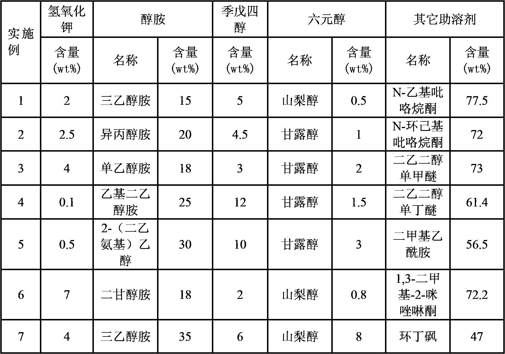
[0021] Prepare the cleaning solution according to the ingredients and proportions of each example in Table 1, and mix them evenly.

[0022] Components and contents of cleaning agents in each example (Examples) of Table 1

[0023]

[0024]

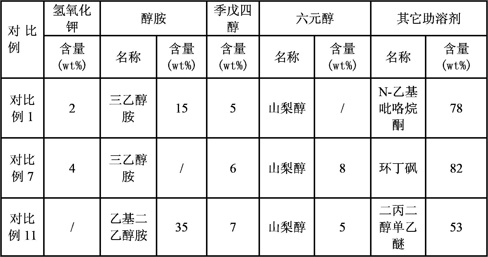
[0025] Component and content of cleaning agent in each comparative example of table 2

[0026]

[0027]

[0028] Wherein, in Comparative Example 7, since no alcohol amine was added, the solution was an incompletely dissolved system.

[0029] In order to further investigate the cleaning situation of this type of cleaning solution, the present invention adopts the following technical means: the wafer containing the positive photoresist (thickness is about 20 microns, and through exposure and etching) is immersed in the cleaning agen...


PUM


Abstract

The invention provides a photoresist cleaning liquid comprising potassium hydroxide, hydramine, pentaerythritol, hexol, and a cosolvent. The cleaning agent has high cleaning capacity, and low corrosion to semiconductor wafer patterns and substrates.

Description

technical field [0001] The invention relates to a photoresist cleaning solution. Background technique [0002] In the usual semiconductor manufacturing process, a photoresist mask is formed on the surface of some materials, and the pattern is transferred after exposure. After the required pattern is obtained, the remaining photoresist needs to be peeled off before the next process. . This process requires complete removal of unwanted photoresist without etching any substrate. [0003] At present, the photoresist cleaning solution is mainly composed of polar organic solvents, strong alkali and / or water, and the photoresist on the semiconductor wafer is removed by immersing the semiconductor wafer in the cleaning solution or rinsing the semiconductor wafer with the cleaning solution. [0004] US5529887 consists of potassium hydroxide (KOH), alkyl glycol monoalkyl ether, water-soluble fluoride and water, etc. to form an alkaline cleaning solution, immerse the wafer in the cle...

Claims


Application Information

Patent Timeline
IPC IPC(8): G03F7/42
Inventor 孙广胜刘兵彭洪修
Owner ANJI MICROELECTRONICS TECH (SHANGHAI) CO LTD
Why Eureka
Try Eureka