Crystalline silicon solar cell and manufacturing method thereof

A technology of a solar cell and a manufacturing method, applied in the field of solar cells, can solve the problems of increasing the short-circuit current of the battery, loss of the battery efficiency, etc., and achieve the effects of reducing surface recombination, increasing the short-circuit current, and increasing the absorption

Inactive Publication Date: 2013-11-13
上海太阳能工程技术研究中心有限公司
View PDF8 Cites 5 Cited by
  • Summary
  • Abstract
  • Description
  • Claims
  • Application Information

AI Technical Summary

Problems solved by technology

Due to the presence of metal impurities on the surface grid lines, recombination will occur on the surface of the battery, resulting in a loss of battery efficiency
If all the thin grid lines and busbars on the front are moved to the back, the short circuit current of the battery will be greatly increased

Method used


Image

  • Crystalline silicon solar cell and manufacturing method thereof
  • Crystalline silicon solar cell and manufacturing method thereof

Examples


Embodiment Construction

[0029] The present invention will be described in detail below in conjunction with the accompanying drawings and specific embodiments.

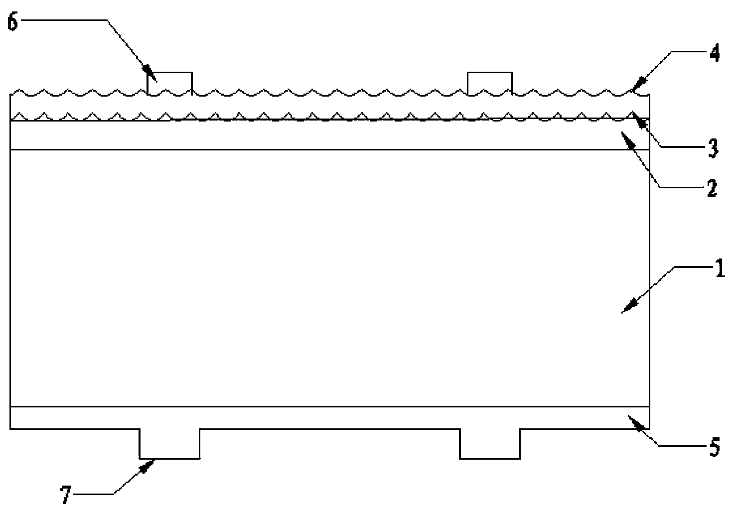
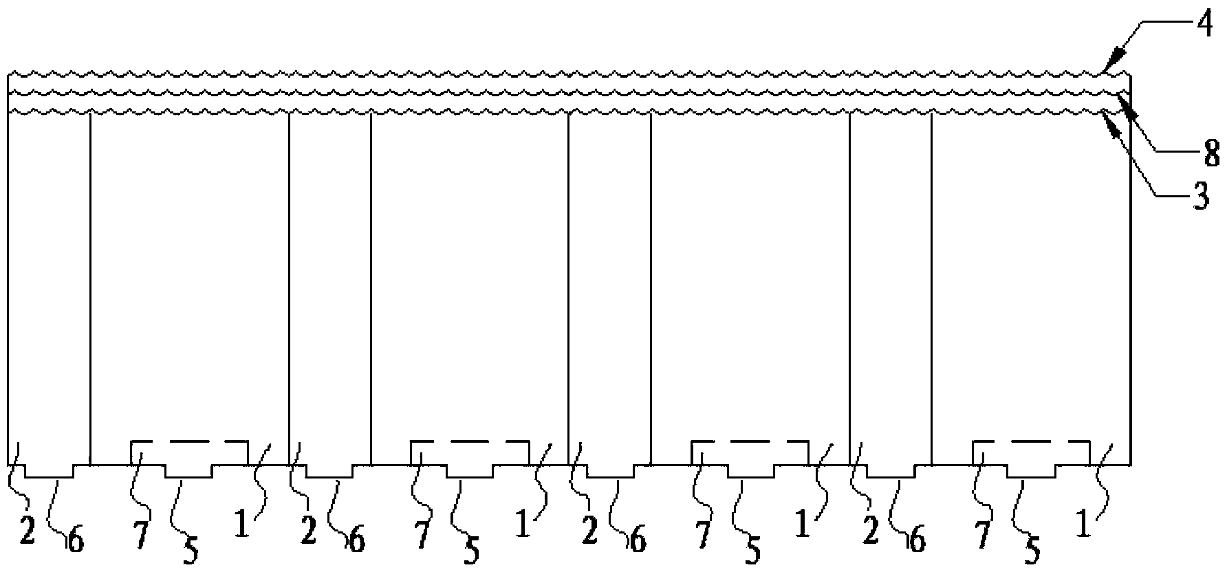
[0030] see figure 2 A kind of crystalline silicon solar cell of the present invention comprises a crystalline silicon wafer substrate, and the crystalline silicon wafer substrate is an N-type or P-type crystalline silicon wafer. A plurality of lateral PN junctions on the end face, and a plurality of lateral PN junctions are connected in series. Each PN junction is composed of a P-type layer 1 and an N-type layer 2, and a textured surface 3 and an anti-reflection layer 4 are sequentially provided on the front surface of the crystalline silicon substrate, and a P region is provided on the back surface of the crystalline silicon substrate. Metal electrode 5 and N-region metal electrode 6 and / or P+ layer 7 .

[0031] The anti-reflection layer in the present invention is SiNx, TiO 2 Thin film or TCO.

[0032] The present invention can also be...


PUM


Abstract

The invention discloses a crystalline silicon solar cell. The crystalline silicon solar cell comprises a crystalline silicon slice substrate. A plurality of transverse PN junctions perpendicular to the end faces of a silicon slice are arranged on the two opposite end faces of the crystalline silicon slice substrate respectively, the PN junctions are composed of P type layers and N type layers respectively, a suede surface and an antireflection layer are sequentially arranged on the front surface of the crystalline silicon slice substrate, and metal electrodes and/or P+ layers are arranged on the back surface of the crystalline silicon slice substrate. A manufacturing method of the crystalline silicon solar cell includes the steps of silicon slice pretreatment, vertical structure treatment, transverse PN junction manufacture, suede surface manufacture, antireflection layer deposition, insulating layer deposition and metallization. According to the crystalline silicon solar cell, incident light loss can be effectively reduced, electrode resistance and contact resistance are reduced, short circuit current, open circuit voltage and fill factors of the solar cell are effectively increased, and conversion efficiency of the solar cell is improved. The crystalline silicon solar cell is high in output voltage and can be used for special occasions.

Description

technical field [0001] The invention relates to a solar cell, in particular to a crystalline silicon solar cell and a manufacturing method thereof. Background technique [0002] At present, conventional industrial crystalline silicon solar cells are composed of a plane PN structure parallel to the surface of the silicon wafer, and the electrodes are respectively located on the front surface and the back surface of the silicon wafer, such as figure 1 shown. As shown in the figure, 1-P-type layer, 2-N-type layer, 3-texture, 4-anti-reflection layer, 5-P region electrode, 6-N region electrode, 7-P+ layer. [0003] The doping layer is parallel to the absorbing layer and located above the absorbing layer, and the incident light first passes through the doping layer and then enters the absorbing layer. Since the doped layer does not contribute to the photogenerated current, the absorption of light by the doped layer should be minimized to reduce light loss. [0004] The area of ...

Claims


Application Information

Patent Timeline
Patent Type & Authority Applications(China)
IPC IPC(8): H01L31/0352H01L31/0224H01L31/0687H01L31/18
CPCY02E10/50Y02E10/544Y02P70/50
Inventor 郭群超庞宏杰王凌云柳琴白晓宇张愿成张滢清
Owner 上海太阳能工程技术研究中心有限公司
Why Eureka
Try Eureka