

Photovoltaic cell and preparation method thereof
A photovoltaic cell and electrode technology, applied in photovoltaic power generation, circuits, electrical components, etc., can solve problems such as silicon-based batteries with high production cost efficiency
- Summary
- Abstract
- Description
- Claims
- Application Information
AI Technical Summary
Problems solved by technology
Method used
Image

Examples
preparation example Construction
[0032] The present invention also provides a method for preparing the above-mentioned photovoltaic cell, comprising:
[0033] performing reactive ion etching on one side of the P-type substrate to obtain a reactive ion etching textured layer;
[0034] Diffusion is carried out in the reactive ion etching textured layer to form a PN junction layer;
[0035] Grooving is performed on the surface of the PN junction layer, and then coating is performed to form an anti-reflection film layer;
[0036] Printing electrode paste on the surface of the anti-reflection film layer to form grid line electrodes;
[0037] The back electrode paste is printed on the surface opposite to the contact surface of the P-type substrate and the reactive ion etching texture layer to form a back electric field and a back electrode.
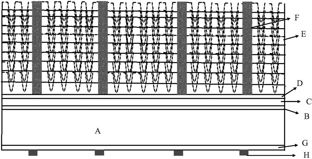
[0038] Wherein, the P-type substrate, the reactive ion etching texture layer, the PN junction layer, the anti-reflection film layer, the grid line electrode, the back electr...
Embodiment 1
[0050] 1.1 Choose 156x156mm polysilicon wafers, the thickness of which is within the range of 210±10μm; clean the silicon wafers before making texture, remove the loss layer and impurities of the original sheet itself, and form a texture layer; the thinning amount is controlled between 0.25 ~ 0.35g .
[0051] 1.2 Put the multi-wafer prepared above into the RIE equipment for reactive ion dry etching to form a reactive ion etching texture layer with a circular hole diameter of 200-500 μm, in which Cl 2 The gas flow is controlled between 400 and 1200 sccm; O 2 The gas flow is controlled between 900 and 2000 sccm; SF 6 The gas input and output flow rates are 600-700sccm and 500-650sccm respectively, the reaction time is 3-5s, the reaction pressure is 24pa, and the power range is between 1000-2000W; the battery is black.
[0052] 1.3 Put the multi-wafer that has been dry-etched into the cleaning equipment for repair. The process is first HF pickling for 120s-deionized water washi...
Embodiment 2
[0060] 2.1 Select 156x156mm polysilicon wafers, the thickness of which is within the range of 210±10μm; the silicon wafers are pre-cleaned and textured to remove the loss layer and impurities of the original wafer itself to form a textured layer; the thinning amount is 0.25g.
[0061] 2.2 Put the multi-wafer prepared above into the RIE equipment for reactive ion dry etching to form a reactive ion etching texture layer with a circular hole diameter of 200-500 μm, in which Cl 2 The flow rate of gas is between 400sccm input and 1200sccm outflow; O 2 Gas flow control is 900sccm; SF 6 The input and output flow rates of the gas are between 600-700sccm and 500-650sccm respectively, the reaction time is 3sec, the reaction pressure is 24pa, and the power range is between 1000W; the battery is black; after this process, the reflectance is measured 9%.
[0062] 2.3 Put the above-mentioned dry-etched multi-chip into the cleaning equipment for repair, the process is first HF pickling for...
PUM
| Property | Measurement | Unit |
|---|---|---|
| Aperture size | aaaaa | aaaaa |
| Depth | aaaaa | aaaaa |
| Width | aaaaa | aaaaa |
Abstract
Description
Claims
Application Information