A led packaged with alsic composite substrate

A composite substrate, LED light source technology, applied in electrical components, circuits, semiconductor devices, etc., can solve the problems of low reactivity of metals and ceramics, poor wettability of metals and ceramics, and high requirements for forming dimensional accuracy, and achieves a suitable size for large Large-scale production, high specific stiffness, and the effect of improving reflectivity

Active Publication Date: 2016-10-05
SOUTH CHINA UNIV OF TECH
View PDF9 Cites 0 Cited by
  • Summary
  • Abstract
  • Description
  • Claims
  • Application Information

AI Technical Summary

Problems solved by technology

Among them, the thermal conductivity of the metal core printed circuit board is limited by the insulating layer, the thermal conductivity is low, and on-board packaging cannot be realized; the copper-clad ceramic board adopts a direct bonding method to bond ceramics and metals together, which improves the thermal conductivity. At the same time, the thermal expansion coefficient is controlled in an appropriate range, but the reaction ability of metal and ceramics is low, and the wettability is not good, which makes the bonding difficult, the interface bonding strength is low, and it is easy to fall off; High dimensional accuracy is required, the process is complex, and there are also problems of poor wettability and easy fall off of metal and ceramics

Method used


Image

  • A led packaged with alsic composite substrate
  • A led packaged with alsic composite substrate

Examples


Embodiment

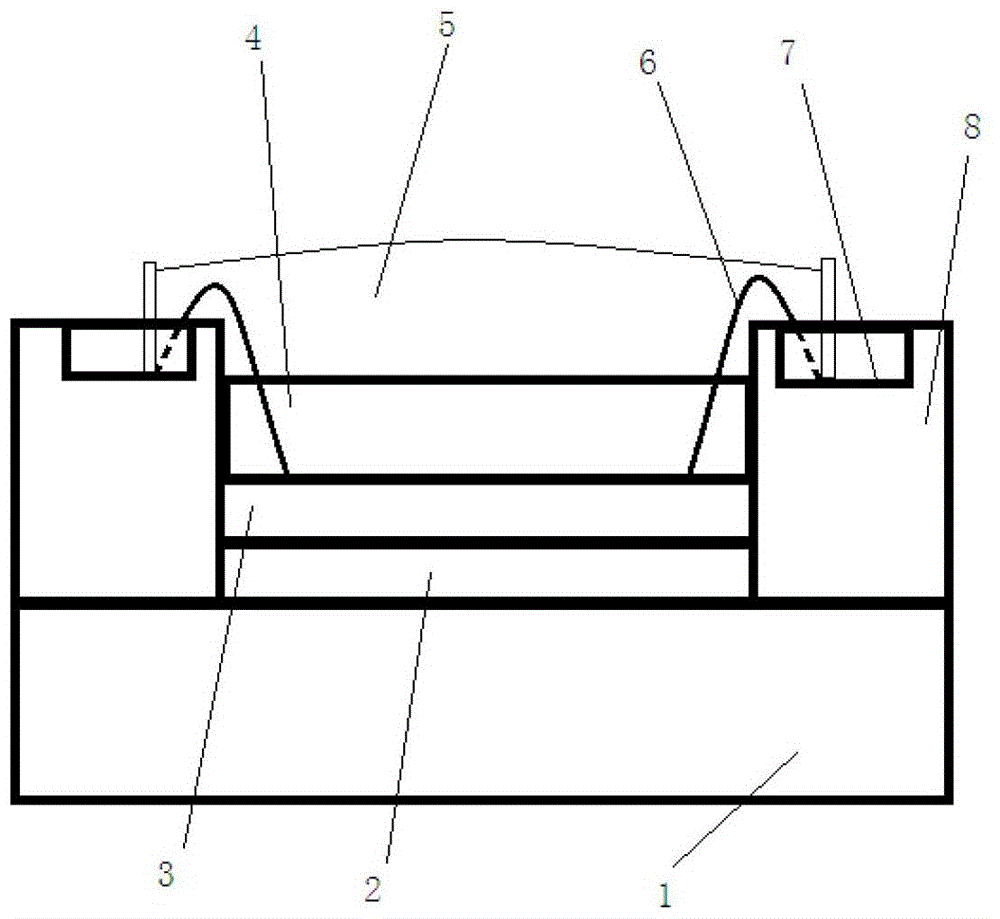
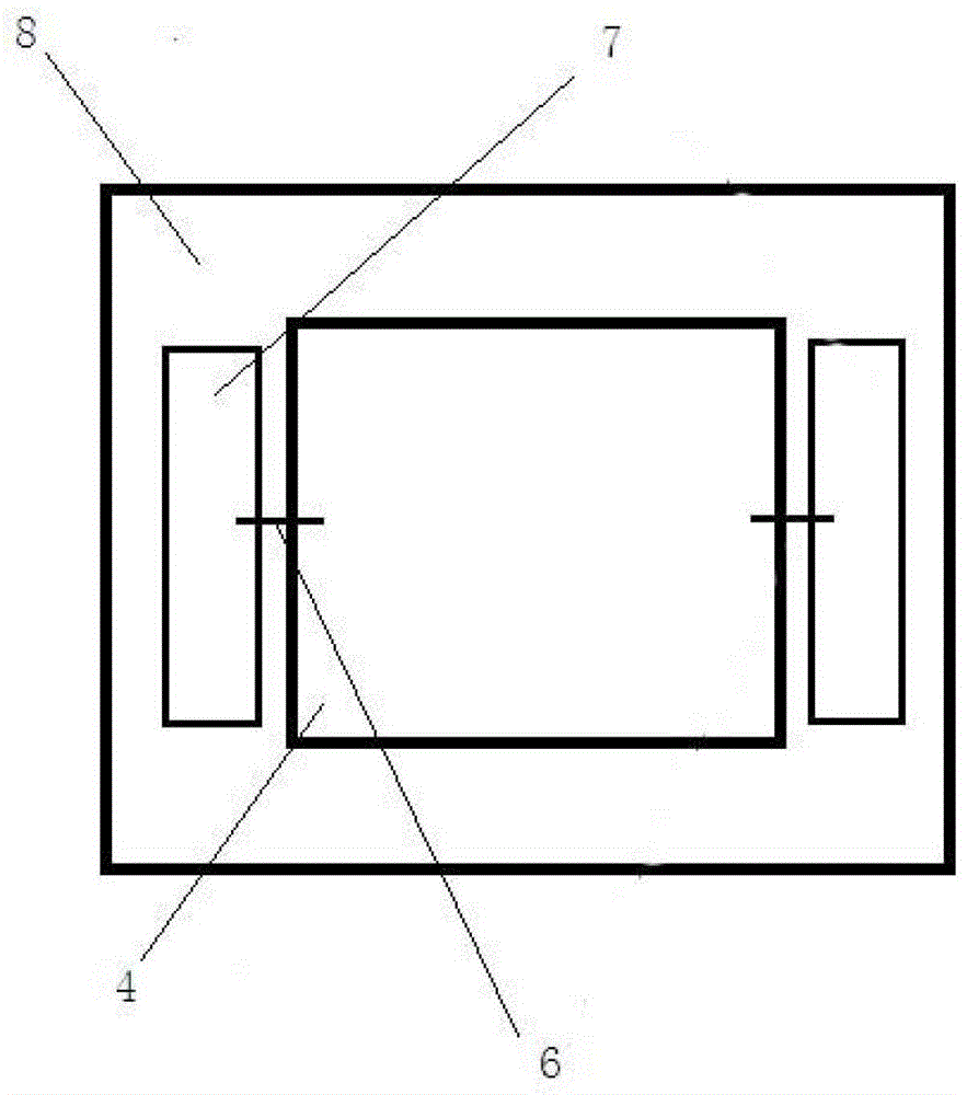
[0020] like Figure 1~2 As shown, an LED packaged with an AlSiC composite substrate in this embodiment includes an AlSiC composite heat dissipation substrate 1 coated with a copper film 2 and a silver film 3 in sequence on the surface, an LED light source module 4, a gold wire 6 and an alumina ceramic frame 8 The LED light source module 4 is packaged on the AlSiC composite heat dissipation substrate 1 using a COB packaging process; the alumina ceramic frame 8 is arranged on the outside of the LED light source module 4 and bonded to the LED light source module 4; the alumina ceramic frame 8 Two copper film electrodes 7 are plated on the top, and the two copper film electrodes 7 are respectively connected to the positive and negative electrodes of the LED light source module 4 through gold wires 6. The transparent silica gel 5 wraps the gold wire 6, and the copper film electrodes 7 are connected to the gold wire 6. part.

[0021] The copper film includes a first layer of copper...

Embodiment 2

[0030] This embodiment is the same as Embodiment 1 except the following features.

[0031] The thickness of the first copper film of the LED packaged with the AlSiC composite substrate in this embodiment is 1 μm, and the thickness of the second layer copper film is 20 μm.


PUM

PropertyMeasurementUnit
thicknessaaaaaaaaaa
thicknessaaaaaaaaaa
thicknessaaaaaaaaaa

Abstract

The invention discloses an LED packaged with an AlSiC composite substrate. The LED comprises the AlSiC composite cooling substrate, an LED light source module, gold threads and an alumina ceramic frame, wherein the surface of the AlSiC composite cooling substrate is plated with a copper film and a silver film sequentially; the LED light source module is packaged on the AlSiC composite cooling substrate; the alumina ceramic frame is arranged on the outer side of the LED light source module and adheres to the LED light source module; two copper-film electrodes are plated on the alumina ceramic frame and connected with a positive pole and a negative pole of the LED light source module through the gold threads respectively. According to the LED, thermal expansion coefficients of the AlSiC composite substrate and an LED chip material are matched, so that an LED chip which is packaged on the substrate is not prone to falling, and the service life of the LED is prolonged.

Description

technical field [0001] The invention relates to an LED packaged on a board, in particular to an LED packaged with an AlSiC composite substrate. Background technique [0002] With the development of microelectronic devices in the direction of high performance, light weight and miniaturization, microelectronics puts forward more and more stringent requirements for packaging materials. Traditional packaging materials include silicon substrates, metal substrates, and ceramic substrates. Silicon and ceramic substrates are difficult to process, high in cost, and low in thermal conductivity; the thermal expansion coefficient of metal materials does not match that of microelectronic chips, which will cause thermal stress and warp during use. Therefore, it is difficult for these traditional packaging materials to meet the demanding requirements of packaging substrates. This is especially important for high power LEDs. [0003] Newly developed heat dissipation substrate materials a...

Claims


Application Information

Patent Timeline
Patent Type & Authority Patents(China)
IPC IPC(8): H01L33/48H01L33/64
Inventor 李国强凌嘉辉刘玫潭刘家成
Owner SOUTH CHINA UNIV OF TECH
Why Eureka
Try Eureka