Low-voltage bandgap-free reference voltage source
A technology of reference voltage source and reference voltage, which is applied in the direction of adjusting electrical variables, control/regulation systems, instruments, etc., to achieve the effects of small process influence, overcoming nonlinear relationship problems, and adjustable output voltage
- Summary
- Abstract
- Description
- Claims
- Application Information
AI Technical Summary
Problems solved by technology
Method used
Image
Examples
Embodiment
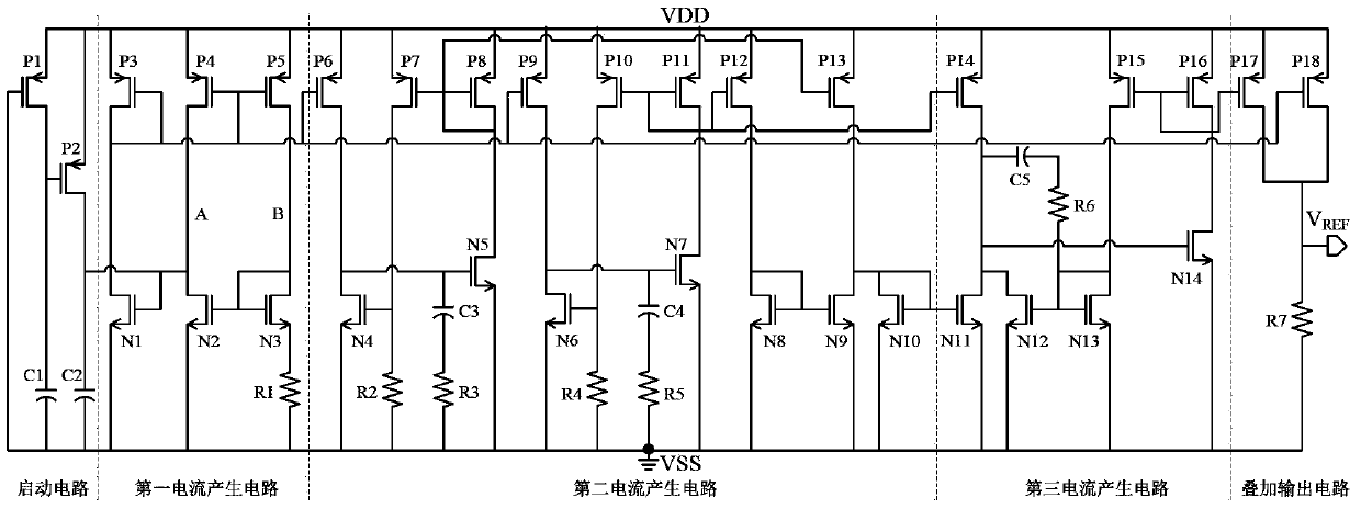
[0017] The circuit structure of this example is as figure 2 As shown, including: 14 NMOS transistors (N1~N14), 18 PMOS transistors (P1~P18), 7 resistors (R1~R7) and 5 capacitors (C1~C5). The specific connection relationship of the circuit is as follows:
[0018]The sources of the PMOS transistors P1~P18 are all connected to the power supply voltage VDD; the gate of the PMOS transistor P1, one end of the capacitor C1, one end of the capacitor C2, one end of the resistors R1~R5, one end of the resistor R7, and the sources of the NMOS transistors N1 and N2 Both poles and the sources of NMOS transistors N4~N14 are grounded at potential VSS; the drain of PMOS transistor P1 and the gate of PMOS transistor P2 are connected to the other end of capacitor C1; the drains of PMOS transistors P2 and P4, and the gate of NMOS transistor N2 The drain of the NMOS transistor N1 and the gate of the NMOS transistor N1 are connected to the other end of the capacitor C2; the gate of the PMOS tran...
PUM
 Abstract
Description
Claims
Application Information


