Epitaxial structure for improving GaN (Gallium Nitride)-based current spreading and growth method thereof

A technology of epitaxial structure and current expansion, which is applied in the direction of circuits, electrical components, semiconductor devices, etc., can solve the problems of crystal quality degradation, carrier scattering, electrical conductivity decline, etc., and achieve the goal of increasing Vz, improving crystal quality, and improving leakage Effect

Inactive Publication Date: 2013-11-20
江苏华功半导体有限公司
View PDF4 Cites 12 Cited by
  • Summary
  • Abstract
  • Description
  • Claims
  • Application Information

AI Technical Summary

Problems solved by technology

However, as the n-type doping concentration increases, the crystal quality decreases, the carrier scattering is severe, and the conductivity decreases, so the problem of current crowding cannot be solved by increasing the n-type doping concentration.

Method used


Image

  • Epitaxial structure for improving GaN (Gallium Nitride)-based current spreading and growth method thereof

Examples


Embodiment Construction

[0018] The embodiments of the present invention are described in detail below: the present embodiment is implemented under the premise of the technical solution of the present invention, and detailed implementation and specific operation process are provided, but the protection scope of the present invention is not limited to the following implementation example.

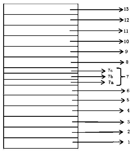
[0019] Such as figure 1 As shown, the epitaxial structure for improving GaN-based current spreading provided by the present invention, from bottom to top, includes: substrate 1, low-temperature GaN buffer layer 2, GaN undoped layer 3, n-type GaN layer n1 layer 4. N-type AlGaN layer 5, n-type GaN layer n2 layer 6, n-type GaN layer LN layer 7, multi-quantum well structure MQW 8, multi-quantum well active layer 9, low-temperature P-type GaN layer 10, P-type AlGaN layer 11. A high-temperature P-type GaN layer 12 and a P-type contact layer 13 .

[0020] The above-mentioned method for growing a gallium nitride-based...


PUM


Abstract

The invention relates to an epitaxial structure for improving GaN (Gallium Nitride)-based current spreading and a growth method thereof. From bottom to top, the epitaxial structure sequentially comprises a substrate, a low-temperature GaN buffer layer, a GaN undoped layer, an n-type GaN layer n1 layer, an n-type AlGaN (Aluminum Gallium Nitride) layer, an n-type GaN layer n2 layer, an n-type GaN layer LN layer, an MQW (Multiple Quantum Well) structure, an MQW active layer, a low-temperature p-type GaN layer, a p-type AlGaN layer, a high-temperature p-type GaN layer and a p-type contact layer. The growth method of the n-type GaN layer LN layer comprises the steps of firstly growing the n-type GaN layer nGaN3-1 layer, then growing the n-type AlGaN layer and finally growing the n-type GaN layer nGaN3-2 layer. The epitaxial structure and the growth method thereof provided by the invention have the advantages that the current can be effectively enabled to be uniformly spread, the crystal quality of an epitaxial layer is improved and the performance of a device is improved.

Description

[0001] technical field [0002] The invention belongs to the technical field of preparation of group III nitride materials, and in particular relates to a gallium nitride-based epitaxial structure and a growth method for improving current spreading. [0003] Background technique [0004] Light Emitting Diode (LED, Light Emitting Diode) is a semiconductor solid-state light-emitting device, which uses a semiconductor PN junction as a light-emitting material, and can directly convert electricity into light. As a GaN-based blue LED is an electric injection light-emitting device, the current spread distribution is very important to the characteristics of the entire device, which will affect the uniformity, reliability, and heat dissipation of the active area of ​​the device. [0005] In order to realize the uniform expansion of the current, the resistance values ​​of the current passing through different paths should be as close as possible. At present, there are two main so...

Claims


Application Information

Patent Timeline
Patent Type & Authority Applications(China)
IPC IPC(8): H01L33/32
Inventor 郭丽彬蒋利民李刚
Owner 江苏华功半导体有限公司
Why Eureka
Try Eureka