Radiating packaging structure of semiconductor power device

A technology of power devices and packaging structures, which is applied in the direction of semiconductor devices, semiconductor/solid-state device parts, electric solid-state devices, etc., to achieve the effect of improving heat dissipation efficiency and effect, fast and uniform heat, and improving heat dissipation effect

Inactive Publication Date: 2013-11-27
SHENZHEN INST OF ADVANCED TECH CHINESE ACAD OF SCI
View PDF24 Cites 27 Cited by
  • Summary
  • Abstract
  • Description
  • Claims
  • Application Information

AI Technical Summary

Problems solved by technology

[0005] Nowadays, with the development of large-scale integrated circuits, the power of power devices has been greatly increased, and the surface heat flux required for cooling large-scale integrated circuits and IGBTs has reached The magnitude of the heat flux of the core of the light water furnace reactor, the heat dissipation effect of the above-mentioned traditional water-cooled radiator can no longer meet the needs of high efficiency and small size of power devices

Method used


Image

  • Radiating packaging structure of semiconductor power device
  • Radiating packaging structure of semiconductor power device
  • Radiating packaging structure of semiconductor power device

Examples


Embodiment 1

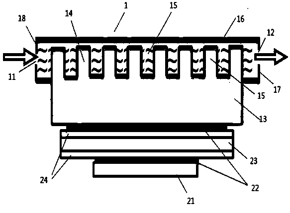
[0032] like figure 1 As shown, the present embodiment provides a heat dissipation packaging structure of an IGBT module, including a heat dissipation housing 1, and the heat dissipation housing 1 is jointly surrounded by a wall 16, a first side wall 17, a second side wall 18 and a cover plate 13. A square shell is formed, wherein the wall 16, the first side wall 17 and the second side wall 18 are integrally formed into an open groove, and a sealing groove (not shown in the figure) is arranged on the edge of the opening groove, and the inside of the sealing groove A sealing ring is provided, and the edge of the cover plate 13 cooperates with the sealing ring to realize the sealing installation between the cover plate 13 and the opening groove, thereby forming a cavity for containing the cooling liquid, wherein the cooling liquid inlet is arranged on the second side wall 18 11. A cooling liquid outlet 12 is provided on the first side wall 17, and the cooling liquid is introduce...

Embodiment 2

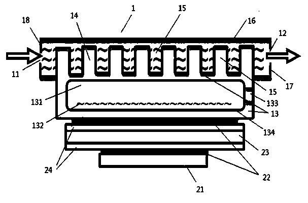
[0037] This embodiment is a modification based on Embodiment 1. Compared with Embodiment 1, the heat dissipation package structure provided by this embodiment is mainly changed in that the structure of the cover plate 13 is changed.

[0038] like figure 2 As shown, the inside of the cover plate 13 is provided with a vacuum cavity 131, the inside of the vacuum cavity 131 is equipped with a liquid phase change medium 132, and the liquid phase change medium 132 is a new fluorocarbon compound, and the vacuum cavity 131 Several capillary structures (not shown in the figure) that facilitate the uniform distribution of the liquid phase change medium 132 are formed on the surface 134 close to the heat transfer direction of the semiconductor power device, that is, grooves. The cross-sectional shape of the capillary structure is triangular. Of course, the cross-sectional shape of the capillary structure may also be trapezoidal or rectangular.

[0039] When the IGBT power device is in ...

Embodiment 3

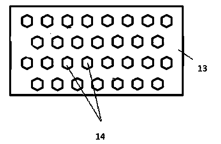
[0043] This embodiment provides a heat dissipation packaging structure for semiconductor power devices, which is a modification of Embodiment 2, and the difference with Embodiment 2 is that the arrangement of the heat dissipation component 14 is changed.

[0044] like Figure 4 As shown, in this embodiment, the cover plate 13 of the heat dissipation housing 1 is provided with six rows of the heat dissipation components 14, and the heat dissipation components 14 in two adjacent rows are arranged in a staggered manner to form a wave-shaped fluid Channel 15 , the wavy fluid channel 15 includes several crests and troughs between adjacent crests, wherein the heat dissipation component 14 is a heat dissipation fin, and the heat dissipation fin is welded on the cover plate 13 .

[0045] Of course, the number of columns of the heat dissipation assembly 14 can be designed in other ways as required, for example, 2 columns, 4 columns, 6 columns, etc.

[0046] When the IGBT power device ...


PUM


Abstract

The invention provides a radiating packaging structure of a semiconductor power device. The radiating packaging structure of the semiconductor power device is provided with a radiating shell body containing cooling liquid, wherein the inner side of a cover plate of the radiating shell body is provided with radiating assemblies and further forms a fluid flow passage, and meanwhile the other side of the cover plate serves as a substrate of the semiconductor power device, namely, the radiating packaging structure and the semiconductor power devices are integrally formed, so the structure is very compact. The radiating packaging structure is characterized in that due to the integrated packaging structure, heat resistance produced by silica gel with a low heat conductivity coefficient is avoided, the radiating assemblies are located on the other side (namely the substrate) of the cover plate, heat from the power device can be directly dissipated, and meanwhile, the radiating effect of the semiconductor power device is greatly improved under the action of turbulent flow of the radiating assemblies.

Description

technical field [0001] The invention relates to a heat dissipation packaging structure of a semiconductor power device, belonging to the technical field of semiconductor heat dissipation. Background technique [0002] Excessive temperature will affect the performance of most semiconductor devices including IGBT modules, and even cause irreversible damage to power devices, affecting the normal use of components. The 10°C rule states that when the device temperature is lowered by 10°C, the reliability of the device will double. Therefore, from the perspective of improving the reliability of semiconductor devices, how to dissipate heat from semiconductor devices has become a research hotspot in various countries. [0003] Take IGBT components as an example. At present, IGBT components in the world are usually air-cooled or water-cooled for heat dissipation after packaging. In traditional water-cooled radiators, the water-cooled plate wall of the water-cooled cavity is connec...

Claims


Application Information

Patent Timeline
Patent Type & Authority Applications(China)
IPC IPC(8): H01L23/473
Inventor 徐国卿刘玢玢李卫民梁嘉宁林桂林常明
Owner SHENZHEN INST OF ADVANCED TECH CHINESE ACAD OF SCI
Why Eureka
Try Eureka