Liquid crystal raster, manufacturing method and driving method thereof and optical phase array device
A liquid crystal grating and driving method technology, applied in optics, nonlinear optics, instruments, etc., can solve the problems of continuous and smooth control of incident light, electric field drop, electrode discontinuity, etc.
- Summary
- Abstract
- Description
- Claims
- Application Information
AI Technical Summary
Problems solved by technology
Method used
Image
Examples
Embodiment 1
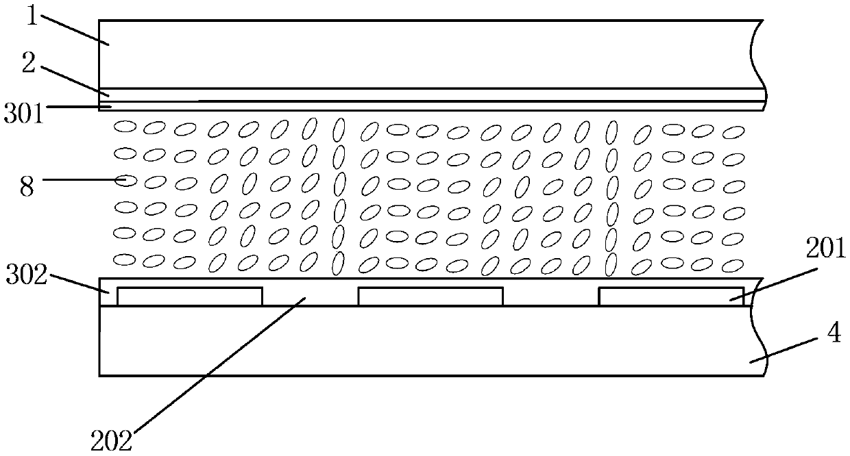
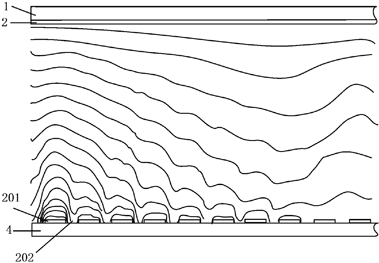
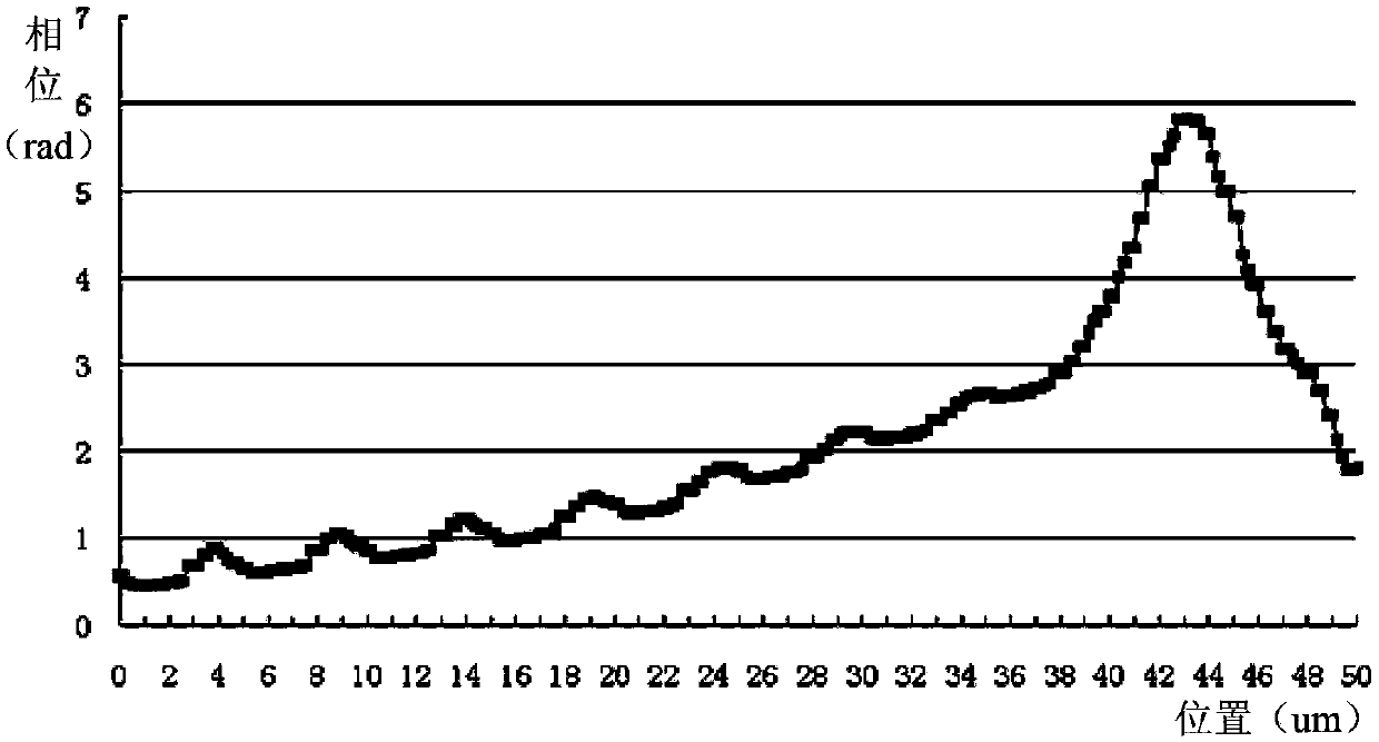
[0034] Figure 4 It is a schematic structural diagram of a liquid crystal grating provided in Embodiment 1 of the present invention, Figure 5 It is a schematic diagram of the electric field equipotential lines inside the liquid crystal grating provided by Embodiment 1 of the present invention, Figure 6 It is a phase curve diagram of incident light controlled by a liquid crystal grating provided in Embodiment 1 of the present invention. Such as Figure 4 to Figure 6 As shown, the liquid crystal grating includes: an upper substrate 1 and a lower substrate 4 oppositely arranged, liquid crystal 8 is filled between the upper substrate 1 and the lower substrate 4, a common electrode 2 is formed on the upper substrate 1, and a plurality of electrodes are formed on the lower substrate 4. The first electrode 6 is formed with a first interval 601 between adjacent first electrodes 6, and a second electrode 7 is arranged above the first interval 601, and a second interval 701 is forme...
Embodiment 2
[0055] Figure 10 The flow chart of the manufacturing method of the liquid crystal grating provided by Embodiment 2 of the present invention, such as Figure 10 As shown, the manufacturing method includes:
[0056] Step 101: forming a common electrode on the upper substrate.
[0057] Step 102: Forming first electrodes on the lower substrate, with a first interval formed between adjacent first electrodes.
[0058] Step 103: forming an insulating layer on the lower substrate on which the first electrode is formed.
[0059] Step 104: forming a second electrode on the lower substrate formed with the insulating layer, the second electrode is located above the first space, and a second space is formed between adjacent second electrodes.
[0060] Step 105: aligning the upper substrate and the lower substrate, and liquid crystal is formed between the upper substrate and the lower substrate.
[0061] Wherein, during cell alignment, the periphery of the liquid crystal cell is bonded...
Embodiment 3
[0065] Embodiment 3 of the present invention provides a method for driving a liquid crystal grating. The liquid crystal grating adopts the liquid crystal grating in Embodiment 1 above. The driving method includes: respectively applying voltages to the first electrode and the second electrode, the first electrode and the common electrode A first electric field is formed between the two electrodes, a second electric field is formed between the second electrode and the common electrode, and the first electric field and the second electric field jointly drive the liquid crystal to deflect.
[0066] Embodiment 3 of the present invention provides a method for driving a liquid crystal grating. The control of the voltage applied to the first electrode and the second electrode is realized through the driving chip. When the voltage is applied to the first electrode and the second electrode, due to the first The combined effect of the electric field and the second electric field produces ...
PUM
 Abstract
Description
Claims
Application Information


