Polarization-doped InN-based tunneling field effect transistor and manufacturing method thereof

A technology of tunneling field effect and polarization doping, which is applied in the direction of diodes, semiconductor/solid-state device manufacturing, semiconductor devices, etc., can solve the problems of increased process complexity, reduced device reliability, and reduced device performance Threshold swing, improved reliability, improved modulation effects

Active Publication Date: 2019-08-20
XI AN JIAOTONG UNIV +1
View PDF5 Cites 4 Cited by
  • Summary
  • Abstract
  • Description
  • Claims
  • Application Information

AI Technical Summary

Problems solved by technology

Devices with this structure, due to the use of traditional physical doping technology, will encounter the same problems as traditional physically doped silicon-based tunneling field effect transistors, such as the inherent high cost of the ion implantation process and its accompanying expensive annealing technology , as well as random doping fluctuation RDFs, the performance of the device is reduced, the complexity of the process is increased, and the reliability of the device is reduced.

Method used


Image

  • Polarization-doped InN-based tunneling field effect transistor and manufacturing method thereof
  • Polarization-doped InN-based tunneling field effect transistor and manufacturing method thereof
  • Polarization-doped InN-based tunneling field effect transistor and manufacturing method thereof

Examples


Embodiment 1

[0062] Embodiment 1: Fabricate a polarization-doped InN-based tunneling field-effect transistor with a polarization inversion layer thickness of 24 nm.

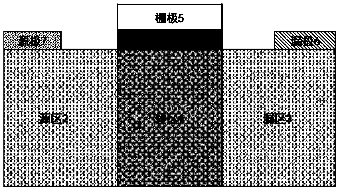
[0063] Step 1. Make a drift layer 2 on the substrate 1, such as image 3 b.

[0064] Using sapphire as the substrate 1, metal organic chemical vapor deposition technology is used to epitaxially unintentionally doped GaN semiconductor material with a thickness of 1000nm in the [0001] crystal direction on the substrate 1 to form a drift layer 2, wherein the process used for epitaxy The conditions are: the temperature is 950° C., the pressure is 40 Torr, the hydrogen gas flow rate is 4000 sccm, the ammonia gas flow rate is 4000 sccm, the gallium source flow rate is 100 μmol / min, and the epitaxy time is 2 h.

[0065] Step 2. Make body region 3, such as image 3 c.

[0066] On the buffer layer 2, the unintentionally doped InN semiconductor material with the [0001] crystal orientation is epitaxed by molecular beam epitaxy techno...

Embodiment 2

[0088] Embodiment 2: Fabricate a polarization-doped InN-based tunneling field-effect transistor with a polarization inversion layer thickness of 10 nm.

[0089] Step 1. Make drift layer 2 on substrate 1, such as image 3 b.

[0090] Using silicon carbide as the substrate 1, metal organic chemical vapor deposition technology is used on the substrate 1 at a temperature of 950°C, a pressure of 40 Torr, a hydrogen flow rate of 4000 sccm, an ammonia gas flow rate of 4000 sccm, and a gallium source flow rate of 100 μmol / min. The drift layer 2 is formed by epitaxially using the unintentionally doped GaN semiconductor material with a thickness of 750 nm in the [0001] crystal orientation under the process condition of an epitaxial time of 1.5 h.

[0091] Step 2. Make body region 3, such as image 3 c.

[0092] On the buffer layer 2, use molecular beam epitaxy technology at a vacuum degree of less than or equal to 1.0×10 -10 mbar, the RF power is 400W, and the reactant is N 2 1. A ...

Embodiment 3

[0114] Embodiment 3: Fabricate a polarization-doped InN-based tunneling field-effect transistor with a polarization inversion layer thickness of 1.2 nm.

[0115] Step A. Make a drift layer 2 on the substrate 1, such as image 3 b.

[0116] GaN material is used as the substrate 1, and the unintentionally doped GaN semiconductor material with a thickness of 500nm in the [0001] crystal orientation is epitaxially used on the substrate 1 by metal-organic chemical vapor deposition technology to form a drift layer 2, wherein the epitaxy adopts The process conditions are: temperature 950°C, pressure 40Torr, hydrogen flow rate 4000sccm, ammonia flow rate 4000sccm, gallium source flow rate 100μmol / min, epitaxy time 1h.

[0117] Step B. Make body region 3, such as image 3 c.

[0118] On the buffer layer 2, use the molecular beam epitaxy technique to epitaxy the unintentionally doped InN semiconductor material with the [0001] crystal orientation to form the bulk region 3 with a thickn...


PUM


Abstract

The invention discloses a polarization-doped InN-based tunneling field effect transistor, and the problem that the random doping fluctuation caused by the conventional physical doping technology leadsto a decrease in device performance, the manufacturing process is complicated and the reliability is low are mainly solved. The polarization-doped InN-based tunneling field effect transistor comprises a substrate (1), a buffer layer (2) and a body region (3) from the bottom to top. An upper right part of the body region is provided with a polarized inversion layer (4), a dielectric layer (8) is deposited on an upper portion of the body region and a left side and an upper portion of the polarized inversion layer, a gate step (9) is etched on the left side of the dielectric layer, a modulationplate (10), a gate electrode (11) and a tunneling gate (12) are orderly deposited on an upper part of the dielectric layer from the right to the left, lower steps (5) are etched at two sides of the body region, and the upper parts of the left and right sides of the steps are provided with a source electrode (7) and a drain electrode (6). According to the invention, the annealing process in the traditional physical doping technology is avoided, the output current and sub-threshold swing of a device are improved, the device reliability is improved, and the polarization-doped InN-based tunnelingfield effect transistor can be used in a low-power circuit system.

Description

technical field [0001] The invention belongs to the technical field of semiconductor devices, and in particular relates to a tunneling field effect transistor which can be used in a low power consumption circuit system. [0002] technical background [0003] With the advancement of technology, the ever-increasing silicon chip area and the shrinking transistor feature size have led to the rapid development of VLSI technology, which has led to the gradual reduction of the manufacturing cost of a single transistor and the continuous improvement of the electrical characteristics of the entire chip. At present, CMOS process technology has entered the 14nm era, and it is still shrinking, advancing towards 7nm and below technology nodes. Today, billions of devices can be integrated on a single chip. However, as the size of transistors shrinks to the nanometer level, problems such as short channel effects become more and more serious, especially the sharp increase in power consumptio...

Claims


Application Information

Patent Timeline
Patent Type & Authority Applications(China)
IPC IPC(8): H01L29/20H01L21/331H01L29/739
CPCH01L29/2003H01L29/66356H01L29/7391
Inventor 王晓飞孙权杨翠
Owner XI AN JIAOTONG UNIV
Why Eureka
Try Eureka