Forming method of semiconductor structure and forming method of MOS transistor

A MOS transistor and semiconductor technology, applied in semiconductor/solid-state device manufacturing, electrical components, circuits, etc., can solve problems such as high doping concentration, in-situ doping, limitations, etc., achieve high concentration uniformity, improve electrical performance effect

Active Publication Date: 2013-12-04
SEMICON MFG INT (SHANGHAI) CORP
View PDF8 Cites 6 Cited by
  • Summary
  • Abstract
  • Description
  • Claims
  • Application Information

AI Technical Summary

Problems solved by technology

[0004] But in situ doping has its limitations
Since the doping concentration of in-situ doping is usually limited by the solid solubility of the material, it cannot reach a very high doping concentration, and may not meet the manufacturing requirements of some semiconductor structures.

Method used


Image

  • Forming method of semiconductor structure and forming method of MOS transistor
  • Forming method of semiconductor structure and forming method of MOS transistor
  • Forming method of semiconductor structure and forming method of MOS transistor

Examples


no. 1 example

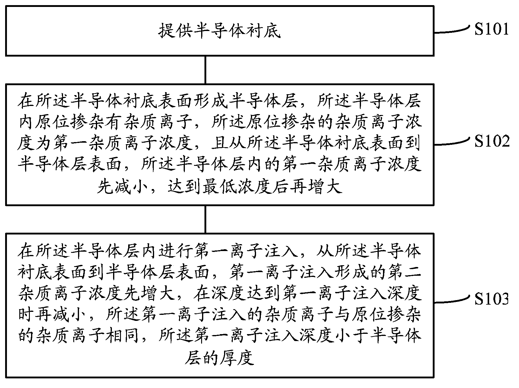
[0046] The first embodiment of the present invention firstly provides a method for forming a semiconductor structure, please refer to figure 2 , is a schematic flowchart of a method for forming a semiconductor structure according to an embodiment of the present invention, specifically including:

[0047] Step S101, providing a semiconductor substrate;

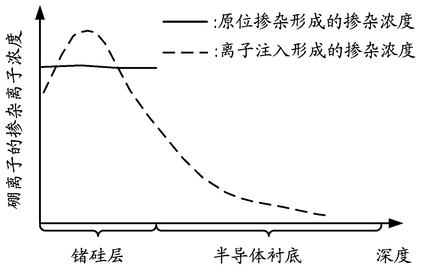
[0048] Step S102, forming a semiconductor layer on the surface of the semiconductor substrate, the semiconductor layer is in-situ doped with impurity ions, the concentration of the in-situ doped impurity ions is a first concentration of impurity ions, and from the semiconductor substrate From the bottom surface to the surface of the semiconductor layer, the concentration of the first impurity ion in the semiconductor layer decreases first, and then increases after reaching the lowest concentration;

[0049] Step S103, performing the first ion implantation in the semiconductor layer, from the surface of the semiconductor subst...

no. 2 example

[0066] The second embodiment of the present invention also provides a method for forming a MOS transistor, please refer to Figure 6 , is a schematic flowchart of a method for forming a MOS transistor according to an embodiment of the present invention, specifically including:

[0067] Step S201, providing a semiconductor substrate, and forming a gate structure on the surface of the semiconductor substrate;

[0068] Step S202, forming trenches in the semiconductor substrate on both sides of the gate structure;

[0069] Step S203, filling the trench with a stress material to form a source / drain region, the source / drain region is in-situ doped with impurity ions, and the concentration of the in-situ doped impurity ions is the third impurity ion Concentration, and from the bottom surface of the source / drain region to the surface of the source / drain region, the concentration of the third impurity ion in the source / drain region decreases first, and then increases after reaching th...


PUM


Abstract

The invention discloses a forming method of a semiconductor structure and a forming method of an MOS transistor. The forming method of the semiconductor structure comprises the steps that a semiconductor substrate is provided; a semiconductor layer is formed on the surface of the semiconductor substrate; from the surface of the semiconductor substrate to the surface of the semiconductor layer, the concentration of first impurity ions in the semiconductor layer decreases at first, reaches the lowest concentration, and then increases; and first ion implantation is carried out in the semiconductor layer by using the same impurity ions, wherein the first ion implantation depth is less than the thickness of the semiconductor layer. From the surface of the semiconductor substrate to the surface of the semiconductor layer, the concentration of second impurity ions formed by ion implantation increases at first, and then decreases, while the concentration of the first impurity ions in-situ doped in the semiconductor layer decreases at first, reaches the lowest concentration, and then increases. The uniformity of the overall concentration formed by adding the concentration of the first impurity ions of all depths in the semiconductor layer and the concentration of the second impurity ions is high, which is conducive to improving the electrical properties of the semiconductor structure.

Description

technical field [0001] The invention relates to the field of semiconductor manufacturing, in particular to a method for forming a semiconductor structure and a method for forming a MOS transistor. Background technique [0002] In the existing semiconductor manufacturing process, ion doping is a very important and common process. Ion doping mainly includes three methods: diffusion, ion implantation and in-situ doping. The first two methods require a high-temperature process, and the ion implantation process may also cause damage to the surface of the semiconductor structure to be implanted, while the in-situ doping is directly doped with the required impurities during the epitaxial growth process. Since the in-situ doping is completed in the epitaxial growth process, no other process is required, especially without high temperature, it can be applied in the formation process of many semiconductor devices, and the in-situ doped dopant ions The concentration is controllable, ...

Claims


Application Information

Patent Timeline
Patent Type & Authority Applications(China)
IPC IPC(8): H01L21/265H01L21/336
Inventor 涂火金何有丰金兰
Owner SEMICON MFG INT (SHANGHAI) CORP
Why Eureka
Try Eureka