

Shock insulator, preparation method of shock insulator and liquid crystal panel
A liquid crystal panel and spacer technology, which is applied in nonlinear optics, instruments, optics, etc., can solve problems such as unstable position, vertical expansion and deformation, and light leakage of display panels, and achieves the effect of simple preparation method and easy realization.
- Summary
- Abstract
- Description
- Claims
- Application Information
AI Technical Summary
Problems solved by technology
Method used
Image

Examples
Embodiment 1
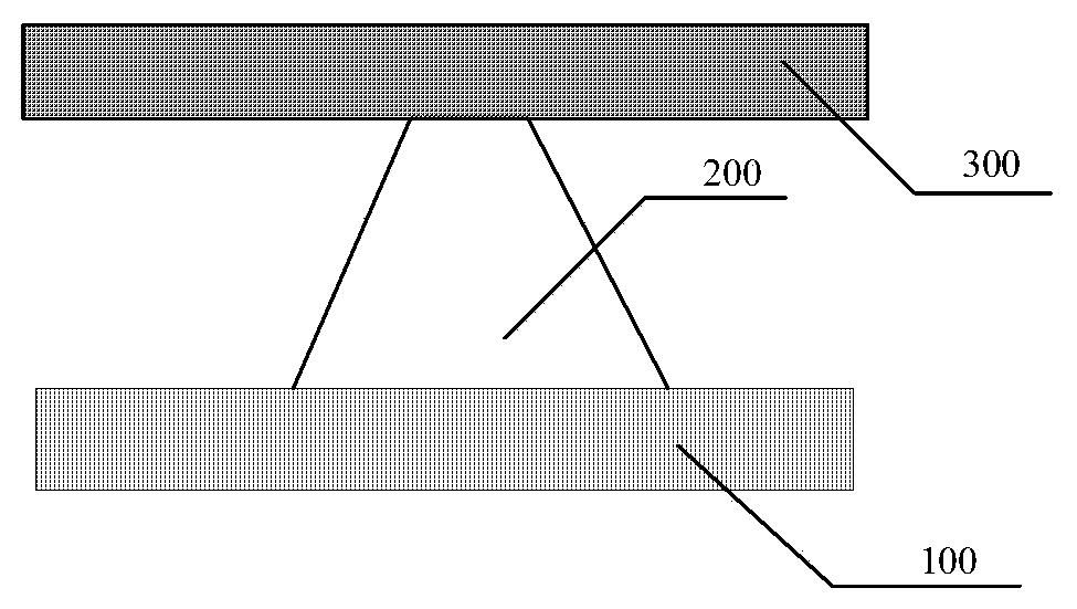
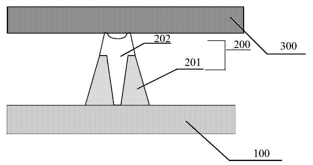
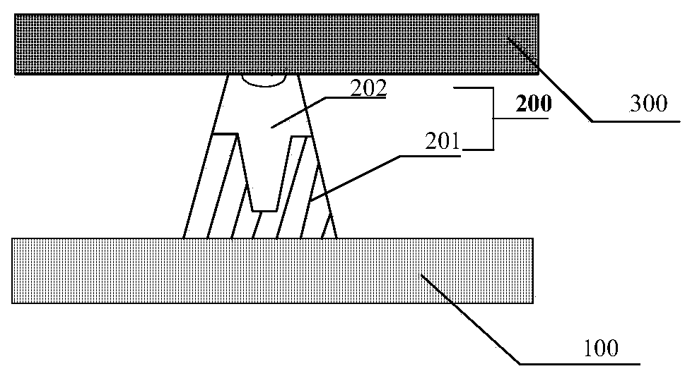
[0035] combine figure 2 , 3 , 4, this embodiment provides a spacer 200, which is arranged between the color filter substrate 100 and the array substrate 300 of the liquid crystal panel, the spacer 200 includes a first component 201 and a second component 202, wherein, The first component 201 is disposed on the array substrate 300 or the color filter substrate 100 , and its height along the vertical central axis is smaller than the height of the spacer 200 (that is to say, the other substrate is in contact with the second component 202 ), The second part 202 is arranged on the first part 201; the first part 201 and the second part 202 are concave-convex structure, and the hardness of the material of the first part 201 is greater than the hardness of the material of the second part 202, and the material of the second part 202 is elastic greater than the elasticity of the material of the first component 201 .
[0036] The material hardness of the first part 201 of the spacer 2...
Embodiment 2
[0046] combine Figure 5 As shown, this embodiment provides a method for preparing the spacer 200 for the spacer 200 described in Embodiment 1, which includes the following steps:
[0047] Step 1: Coating the material layer of the first component on the array substrate 300 or the color filter substrate 100, and forming a pattern including the first component 201 through a patterning process (exposure, development, etching, etc.), wherein the material of the first component 201 The material of the layer is a material with relatively high hardness such as aluminum, molybdenum, silicon oxide, silicon nitride, and indium tin oxide. The height of the first component 201 along the vertical central axis may be controlled by the thickness of the coated first component material layer.
[0048] Step 2: Coating the second component material layer on the substrate formed with the first component 201, and forming a pattern including the second component 202 through a patterning process, w...
Embodiment 3
[0058] This embodiment provides another preparation method for the spacer 200 described in Embodiment 1, which includes the following steps:
[0059] forming a pattern including the first component 201 on the first substrate, the first substrate being the array substrate 300 or the color filter substrate 100;
[0060] A pattern including the second component 202 is formed on the second substrate, which is the array substrate 300 or the color filter substrate 100 .
[0061] That is to say, the first component 201 is formed on the array substrate 300, and the second component 202 is formed on the color filter substrate 100; or the first component 201 is formed on the color filter substrate 100, and the second component 202 is formed on the array substrate 300, Finally, the two substrates are boxed, and the spacer 200 is formed between the two substrates.
[0062] Finally, the first substrate and the second substrate are boxed together, that is to say, the color filter substrate...
PUM
 Abstract
Description
Claims
Application Information