Laminated sheet type bypass wave absorbing device and manufacturing method thereof

A manufacturing method and wave absorber technology, applied in impedance networks, electrical components, multi-terminal pair networks, etc., can solve the problems of difficulty in making larger, weakening effect, and small inductance, so as to suppress electromagnetic interference and improve anti-interference ability. Effect

A manufacturing method and wave absorber technology, applied in impedance networks, electrical components, multi-terminal pair networks, etc., can solve the problems of difficulty in making larger, weakening effect, and small inductance, so as to suppress electromagnetic interference and improve anti-interference ability. Effect

CN103441744AActive Publication Date: 2013-12-11SHENZHEN ZHENHUA FU ELECTRONICS

Image

  • Laminated sheet type bypass wave absorbing device and manufacturing method thereof
  • Laminated sheet type bypass wave absorbing device and manufacturing method thereof
  • Laminated sheet type bypass wave absorbing device and manufacturing method thereof

Examples


Embodiment Construction

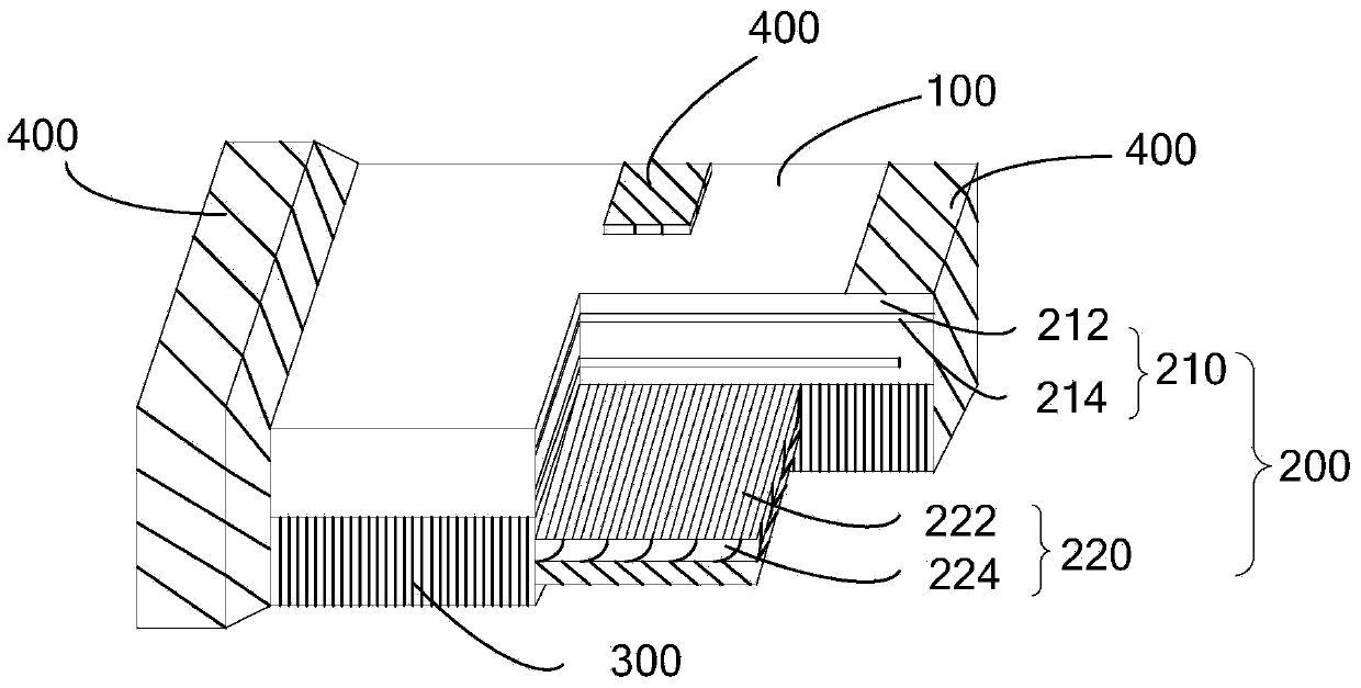
[0039] Such as figure 1 As shown, it is a sectional view of a laminated chip bypass absorber of an embodiment. The laminated chip bypass absorber includes a first cover 100 , an intermediate layer 200 and a second cover 300 . Wherein the first cover 100 is a dielectric ceramic material diaphragm, the middle layer 200 includes a chip capacitor unit 210 and a chip inductor functional device unit 220, and the chip capacitor unit 210 and the chip inductor unit 220 are laminated in parallel. The layers are integrated in a laminated chip monolith. The chip capacitor cell 210 includes a dielectric ceramic material diaphragm 212 and the internal electrode 214 printed on it, and correspondingly the chip inductor functional device cell 220 includes a ferrite material diaphragm 222 and the internal electrode 224 printed on it. , the second cover 300 is a ferrite material diaphragm.

[0040] It can be understood that the positions of the first cover 100 and the second cover 300 can be ...


PUM


Abstract

The invention discloses a laminated sheet type bypass wave absorbing device which comprises a first cover body, a middle layer and a second cover body, wherein the first cover body, the middle layer and the second cover body are sequentially laminated. The middle layer comprises a sheet type capacitor unit and a sheet type inductance function device unit which are laminated in parallel. The invention further discloses a manufacturing method of the laminated sheet type bypass wave absorbing device. The laminated sheet type bypass wave absorbing device and the manufacturing method can meet the wave filtering requirements in different frequency bands, and the slope of an insertion loss characteristic curve is steeper. Compared with a wave absorbing device with a single capacitor or a single inductor, the laminated sheet type bypass wave absorbing device can more effectively absorb noise waves in an electronic circuit and restrain electromagnetic interference of the electronic circuit, and the interference resistant capacity of an electronic device and the reliability of a system are improved.

Description

technical field [0001] The invention relates to the technical field of electronic components, in particular to a laminated chip bypass absorber and a manufacturing method thereof. Background technique [0002] With the continuous advancement of science and technology and the gradual improvement of human living standards, household electrical appliances, mobile and personal portable electronic devices are increasing day by day. In the process of using electronic equipment, electronic equipment will interact and interfere with each other, causing damage to integrated circuits and semiconductor devices. The key to solving this problem is the noise suppression and bypass decoupling of digital IC power supplies. [0003] Traditional digital IC power supply noise suppression and bypass decoupling mostly use ceramic capacitors to decouple noise suppression. Its insertion loss characteristic curve is relatively flat, and the weakening effect is poor when the noise is too large. Con...

Claims


Application Information

Patent Timeline
11 Dec 2013
Publication
CN103441744A
IPC
H03H7/01
Inventors
樊应县; 徐鹏飞