
Manufacturing method of closed cavity of micro-electromechanical system (MEMS)

A manufacturing method and a technique for closing a cavity, which are applied in the manufacture of microstructure devices, techniques for producing decorative surface effects, and decorative art, can solve problems such as long processing cycles, high costs, and interface holes, and reduce production cycles , avoid interface holes, and reduce the effect of minimum size

Inactive Publication Date: 2013-12-18
ADVANCED SEMICON MFG CO LTD
View PDF9 Cites 6 Cited by
  • Summary
  • Abstract
  • Description
  • Claims
  • Application Information

AI Technical Summary

Problems solved by technology

[0008] The purpose of the present invention is to provide a method for manufacturing a MEMS closed cavity, which does not need to use a silicon wafer bonding process, and solves the problems of high cost, long processing cycle and easy silicon-silicon bonding caused by CSOI production in the prior art. Interface holes and other issues

Method used


Image

  • Manufacturing method of closed cavity of micro-electromechanical system (MEMS)
  • Manufacturing method of closed cavity of micro-electromechanical system (MEMS)
  • Manufacturing method of closed cavity of micro-electromechanical system (MEMS)

Examples


Embodiment Construction

[0032] In order to make the content of the present invention clearer and easier to understand, the content of the present invention will be further described below in conjunction with the accompanying drawings. Of course, the present invention is not limited to this specific embodiment, and general replacements known to those skilled in the art are also covered within the protection scope of the present invention.

[0033] Secondly, the present invention is described in detail by means of schematic diagrams. When describing the examples of the present invention in detail, for the convenience of illustration, the schematic diagrams are not partially enlarged according to the general scale, which should not be used as a limitation of the present invention.

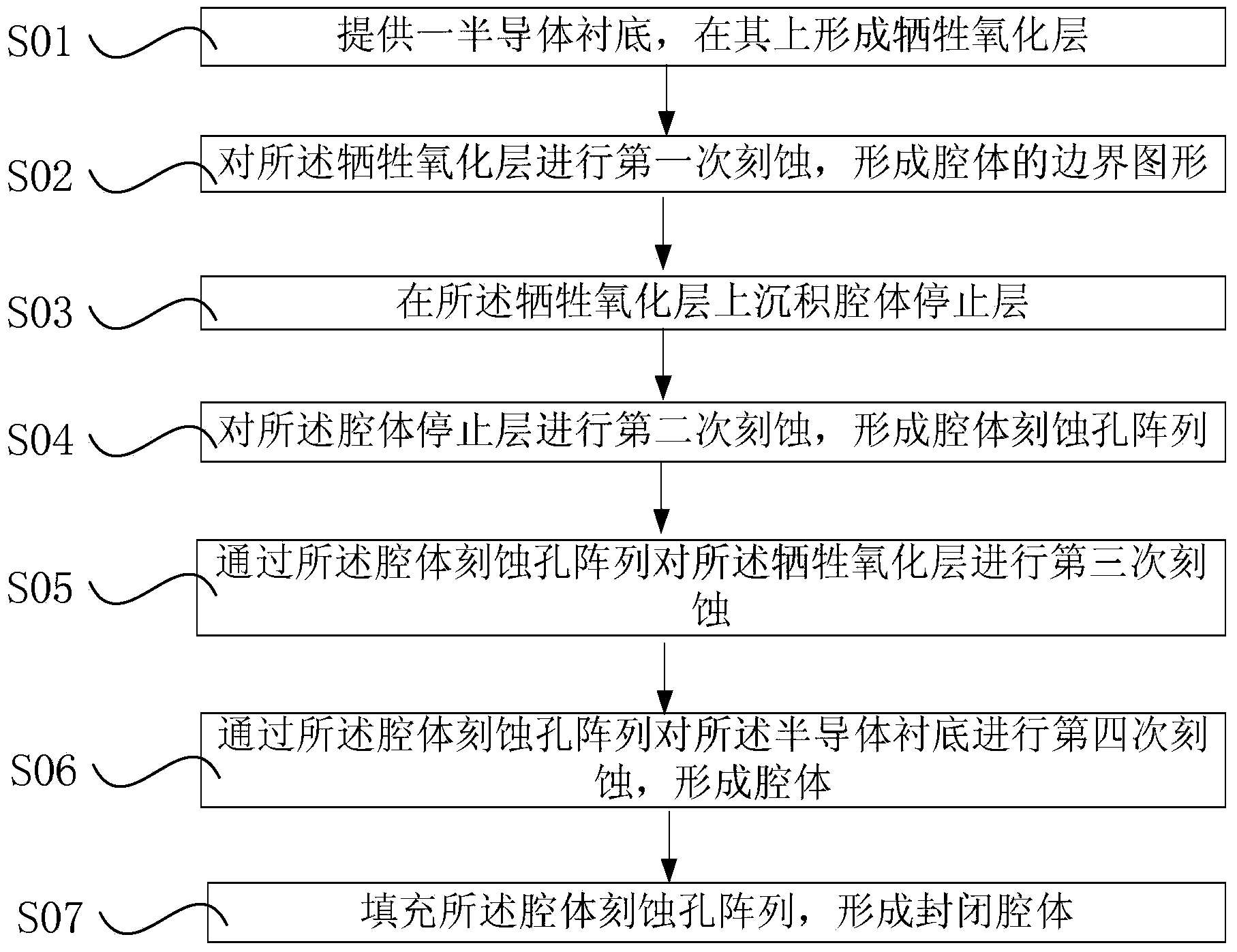
[0034] figure 1 It is a flow chart of the manufacturing process of the MEMS closed cavity in an embodiment of the present invention, such as figure 1 As shown, the present invention proposes a method for manufacturing a MEM...


PUM


Abstract

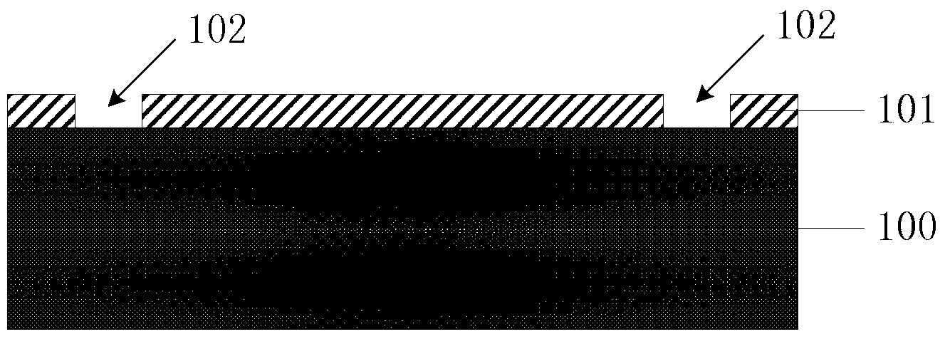
The invention provides a manufacturing method of a closed cavity of a micro-electromechanical system (MEMS). The manufacturing method comprises the steps: forming a sacrificial oxidation layer on a semiconductor substrate, and etching the sacrificial oxidation layer to form a cavity boundary figure; depositing a stop layer of the cavity, and etching the cavity stop layer to form a cavity etching hole array; etching the sacrificial oxidation layer and the semiconductor substrate by the cavity etching hole array to form a cavity; filling the cavity etching hole array to form the closed cavity. The cavity stop layer is deposited on the semiconductor substrate, the sacrificial oxidation layer is formed on the semiconductor substrate, the sacrificial oxidation layer and the semiconductor substrate are etched by the cavity etching hole array formed on the cavity stop layer, so that the cavity is formed; and therefore, the minimum size of the cavity can greatly reduced to a certain extent, the minimum thickness of a top dielectric layer is reduced, a silicon wafer bonding process is omitted, the problems of interfaces holes and the like can be avoided, and the reliability of a device can be improved.

Description

technical field [0001] The invention relates to the technical field of micro-electromechanical systems, in particular to a method for manufacturing a MEMS closed cavity. Background technique [0002] At present, as a semiconductor substrate that can improve the performance of semiconductor devices, SOI (Silicon on Insulator, silicon on insulator) has been widely valued. SOI is a conventional single crystal silicon wafer embedded with a layer of insulating silicon dioxide. A new type of semiconductor silicon material formed from silicon, including a silicon substrate, an insulating layer and a top silicon layer. In the prior art, the methods for manufacturing SOI materials mainly include: [0003] Ion implantation technology: Using the principle of ion implantation of oxygen, oxygen ions are implanted under the surface of the silicon wafer, and a layer of buried oxide layer is formed through annealing treatment, so as to obtain a top silicon layer on the insulating silicon s...

Claims


Application Information

Patent Timeline
Patent Type & Authority Applications(China)
IPC IPC(8): B81C1/00
Inventor 徐元俊杨海波郑欢
Owner ADVANCED SEMICON MFG CO LTD
Learn More