Thin film transistor, manufacturing method thereof, array substrate and display device

A technology of thin-film transistors and array substrates, which is applied in the field of liquid crystal display, and can solve problems such as reduced display effect, large parasitic capacitance, and increased floating pixel voltage.

Inactive Publication Date: 2013-12-18
HEFEI BOE OPTOELECTRONICS TECH +1
View PDF3 Cites 12 Cited by
  • Summary
  • Abstract
  • Description
  • Claims
  • Application Information

AI Technical Summary

Problems solved by technology

[0005] The prior art has the following problems: figure 1 In the structure shown, the parasitic capacitance between the source electrode and the gate electrode of the TFT is relatively large, and the parasi

Method used


Image

  • Thin film transistor, manufacturing method thereof, array substrate and display device
  • Thin film transistor, manufacturing method thereof, array substrate and display device
  • Thin film transistor, manufacturing method thereof, array substrate and display device

Examples


Embodiment Construction

[0038] In order for those skilled in the art to better understand the technical solution of the present invention, a thin film transistor, a manufacturing method thereof, an array substrate and a display device provided by the present invention will be further described in detail below with reference to the accompanying drawings.

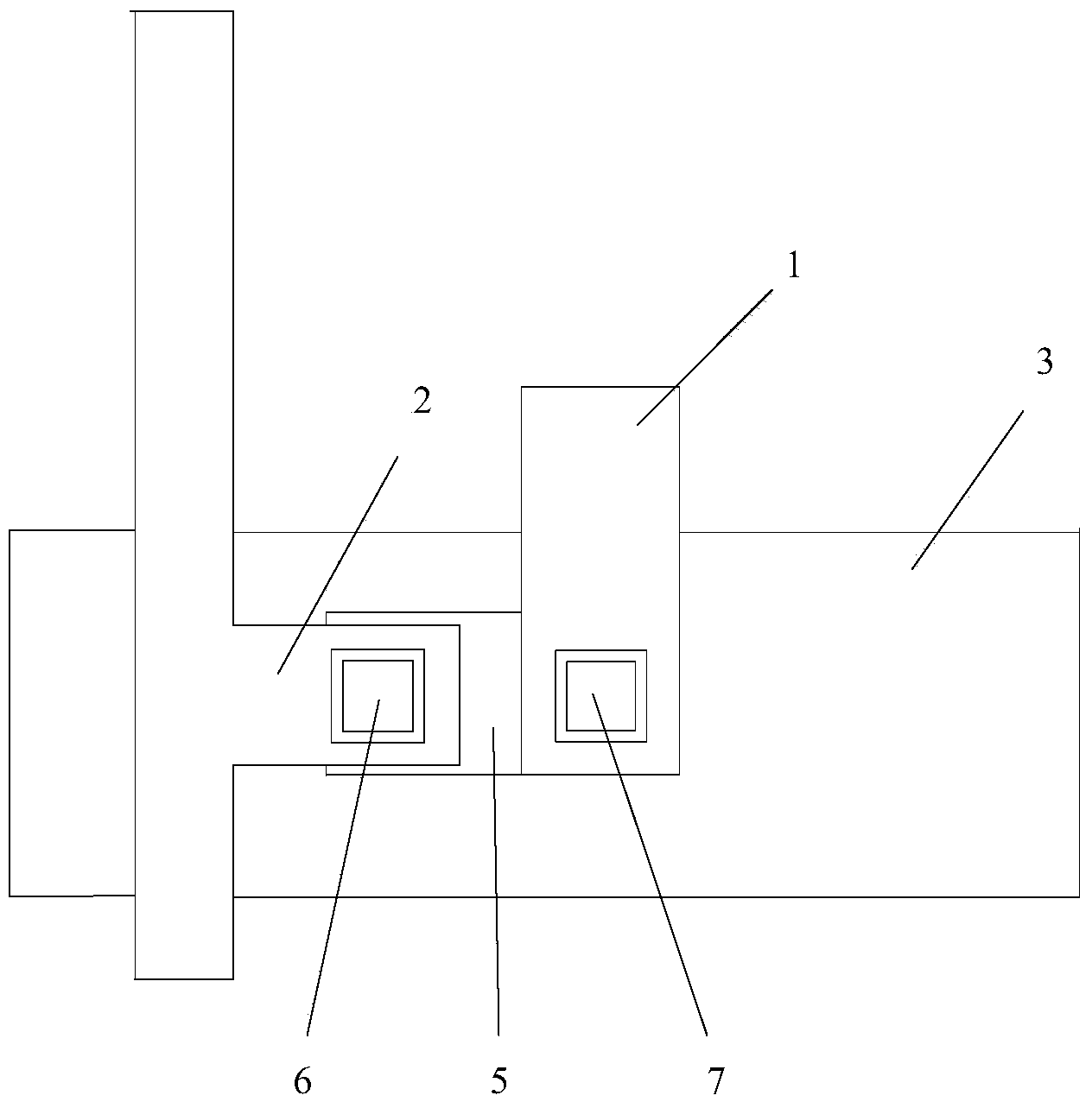
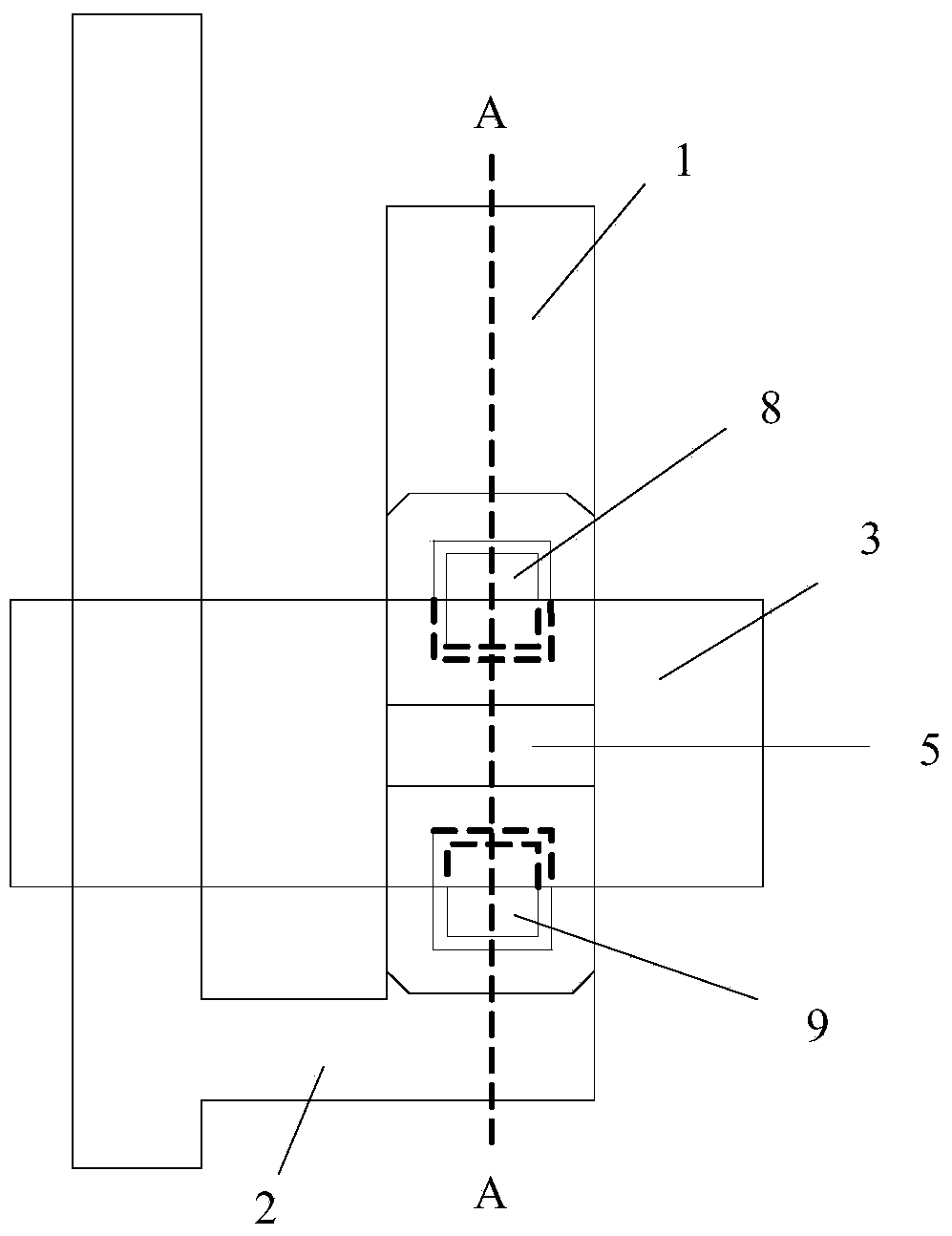
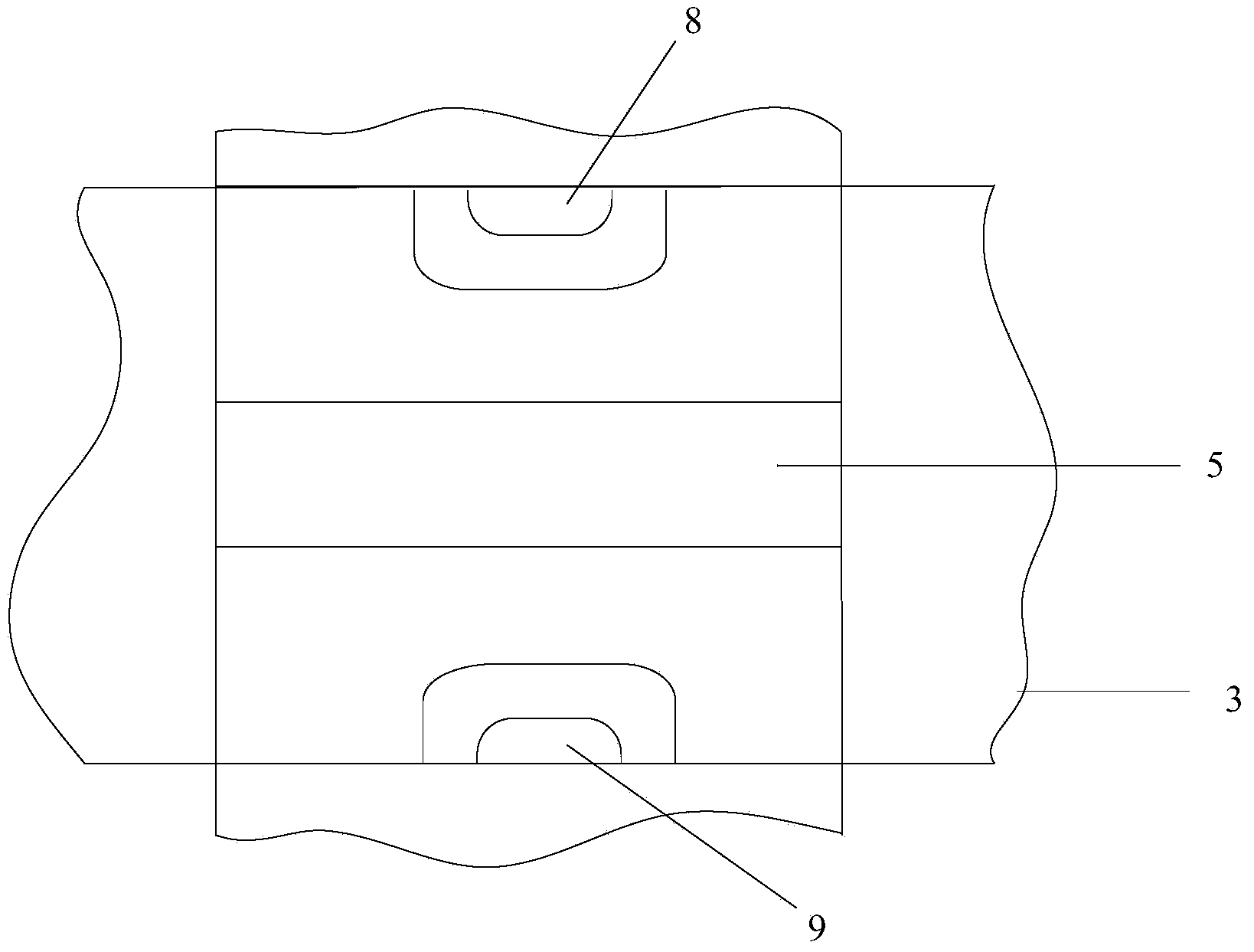
[0039] figure 2 It is a schematic top view of a thin film transistor provided in Embodiment 1 of the present invention, image 3 for figure 2 Schematic diagram of the cross-sectional structure of a thin film transistor, such as figure 2 and image 3 As shown, the thin film transistor includes: a gate electrode 3, an active layer 4, an etching barrier layer 5, a source electrode 1 and a drain electrode 2, and the etching barrier layer 5 is arranged on the active layer 4 and the source electrode 1 and the drain electrode 2 The first via hole 8 and the second via hole 9 are arranged between them, the source electrode 1 is connected to the active ...


PUM


Abstract

The invention provides a thin film transistor, a manufacturing method of the thin film transistor, an array substrate and a display device. The thin film transistor comprises a gate electrode, an active layer, an etching barrier layer, a source electrode and a drain electrode, wherein the etching barrier layer is arranged among the active layer, the source electrode and the drain electrode, and is provided with a first through hole and a second through hole, the source electrode is connected with the active layer through the first through hole, the drain electrode is connected with the active layer through the second through hole, and the gate electrode coincides with part of the first through hole and part of the second through hole, and coincides with a portion between the first through hole and the second through hole. According to the technical scheme, the frequency of the phenomenon that pixel voltage floats can be reduced, and the display effect can be improved.

Description

technical field [0001] The invention relates to the technical field of liquid crystal display, in particular to a thin film transistor, a manufacturing method thereof, an array substrate and a display device. Background technique [0002] Thin Film Transistor Liquid Crystal Display (English: Thin Film Transistor Liquid Crystal Display, referred to as: TFT-LCD) has become a mainstream product in the market due to its advantages of high image quality, high space utilization, low power consumption, and no radiation. The TFT liquid crystal display is to design at least one TFT on each pixel point, and each independent pixel on the screen is controlled through the TFT, which can greatly improve the response time. [0003] Indium Gallium Zinc Oxide (IGZO) is a new generation of material used in the active layer of TFT, its carrier mobility is 5 to 10 times that of amorphous silicon, which can greatly improve the charge and discharge speed of the pixel electrode , improve pixel re...

Claims


Application Information

Patent Timeline
IPC IPC(8): H01L29/786H01L21/336
CPCH01L27/124H01L21/02565H01L21/441H01L21/76802H01L21/76832H01L23/5226H01L23/528H01L23/53295H01L27/1259H01L29/24H01L29/41733H01L29/4175H01L29/42384H01L29/66969H01L29/78606H01L29/7869H01L2924/0002
Inventor 杨海鹏尹傛俊涂志中金在光
Owner HEFEI BOE OPTOELECTRONICS TECH
Why Eureka
Try Eureka