Multi-layer circuit board and manufacturing method thereof

A technology of a multilayer circuit board and a manufacturing method, which is applied in the direction of multilayer circuit manufacturing, printed circuit components, etc., can solve the problems of reducing circuit design area, affecting the yield and quality of circuit boards, and large thickness of embedded circuit boards.

Active Publication Date: 2013-12-18
QI DING TECHNOLOGY QINHUANGDAO CO LTD +1
View PDF4 Cites 17 Cited by
  • Summary
  • Abstract
  • Description
  • Claims
  • Application Information

AI Technical Summary

Problems solved by technology

However, on the one hand, because the existence of the groove reduces the area of ​​the circuit design, the embedded circuit board may have a relatively large thickness; It will affect the yield and quality of the circuit board

Method used


Image

  • Multi-layer circuit board and manufacturing method thereof
  • Multi-layer circuit board and manufacturing method thereof
  • Multi-layer circuit board and manufacturing method thereof

Examples


Embodiment Construction

[0033] The multilayer circuit board provided by the technical solution and its manufacturing method will be further described in detail below in conjunction with the drawings and multiple embodiments.

[0034] The method for manufacturing a multilayer circuit board provided by the first embodiment of the technical solution includes steps:

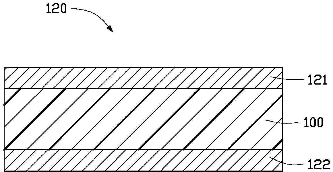
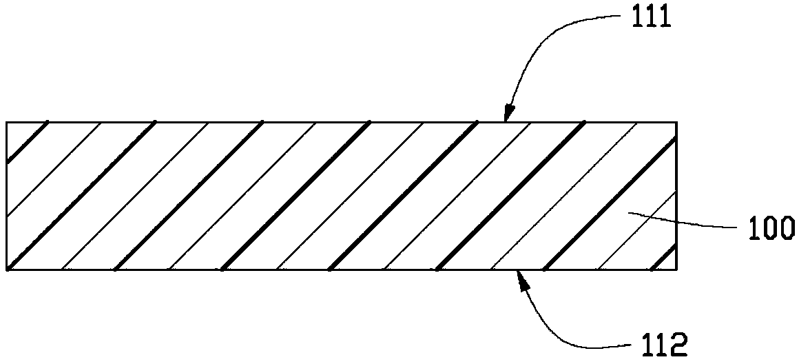
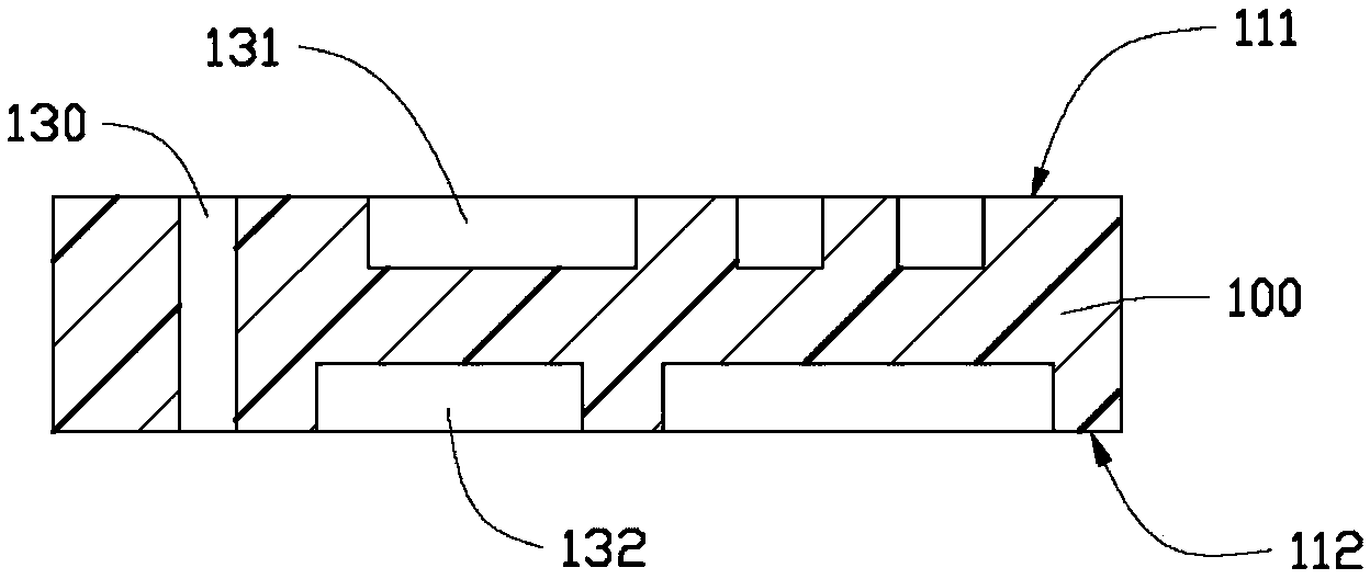
[0035] For the first step, please also refer to figure 1 and figure 2 , an insulating substrate 100 is provided, and the insulating substrate 100 has a first surface 111 and a second surface 112 opposite to each other.

[0036] The insulating base 100 may be a purchased insulating sheet, or may be made by etching a purchased copper-clad substrate. In this embodiment, the insulating base 100 is formed through the following steps: First, a double-sided copper-clad substrate 120 is provided, and the double-sided copper-clad substrate 120 includes the insulating base 100 and the The upper copper foil 121 and the lower copper foil 122 ; seco...


PUM


Abstract

The invention provides a manufacturing method of a multi-layer circuit board. The method includes providing an insulation substrate provided with a corresponding first surface and second surface; forming a through hole penetrating the first surface and the second surface on the insulation substrate, a first blind groove only exposing on the first surface and a second blind groove only exposing on the second surface; depositing conductive material on the insulation substrate to form a conductive hole embedded in the insulation substrate, a first circuit pattern, provided with an assembling area and a pressing area, flush with the first surface and a second circuit pattern flush with the second surface; forming a first pressed substrate plate, comprising a first conductive circuit layer and a first film, on the first surface to obtain a multi-layer substrate plate; removing the first pressed substrate plate corresponding to the assembling area, forming an outer-exposing groove in the multi-layer substrate plate, and allowing the assembling area to expose in the groove. The invention further provides a multi-layer circuit board manufactured by the method.

Description

technical field [0001] The invention relates to circuit board technology, in particular to a multilayer circuit board with grooves and a manufacturing method thereof. Background technique [0002] In the information, communication and consumer electronics industries, circuit boards are an indispensable and basic component of all electronic products. With the development of electronic products in the direction of miniaturization and high speed, circuit boards are also developing from single-sided circuit boards to double-sided circuit boards and multi-layer circuit boards. Multilayer circuit boards, especially multilayer circuit boards with embedded electronic components, are widely used. Please refer to the literature published by Takahashi, A. et al. in IEEE Trans. on Components, Packaging, and Manufacturing Technology in 1992 "High density multilayer printed circuit board for HITAC M~880". [0003] A multilayer circuit board with embedded electronic components generally ...

Claims


Application Information

Patent Timeline
Patent Type & Authority Applications(China)
IPC IPC(8): H05K3/46H05K1/02
Inventor 许哲玮许诗滨
Owner QI DING TECHNOLOGY QINHUANGDAO CO LTD
Why Eureka
Try Eureka