Semiconductor manufacturing device and manufacturing method thereof

A technology for manufacturing devices and manufacturing methods, applied to semiconductor manufacturing devices and manufacturing fields, capable of solving problems such as increased power usage and reduced signal transmission speed of semiconductor components, and achieving the effects of preventing increased power usage, reducing signal transmission speed, and preventing oxidation

Inactive Publication Date: 2013-12-18
WONIK IPS CO LTD
View PDF6 Cites 2 Cited by
  • Summary
  • Abstract
  • Description
  • Claims
  • Application Information

AI Technical Summary

Problems solved by technology

Oxidation of copper causes problems such as increased power usage of semiconductor elements and decreased signal transmission speed as contact resistance increases

Method used


Image

  • Semiconductor manufacturing device and manufacturing method thereof
  • Semiconductor manufacturing device and manufacturing method thereof
  • Semiconductor manufacturing device and manufacturing method thereof

Examples


Embodiment Construction

[0019] Preferred embodiments of the present invention will be described in detail below with reference to the accompanying drawings.

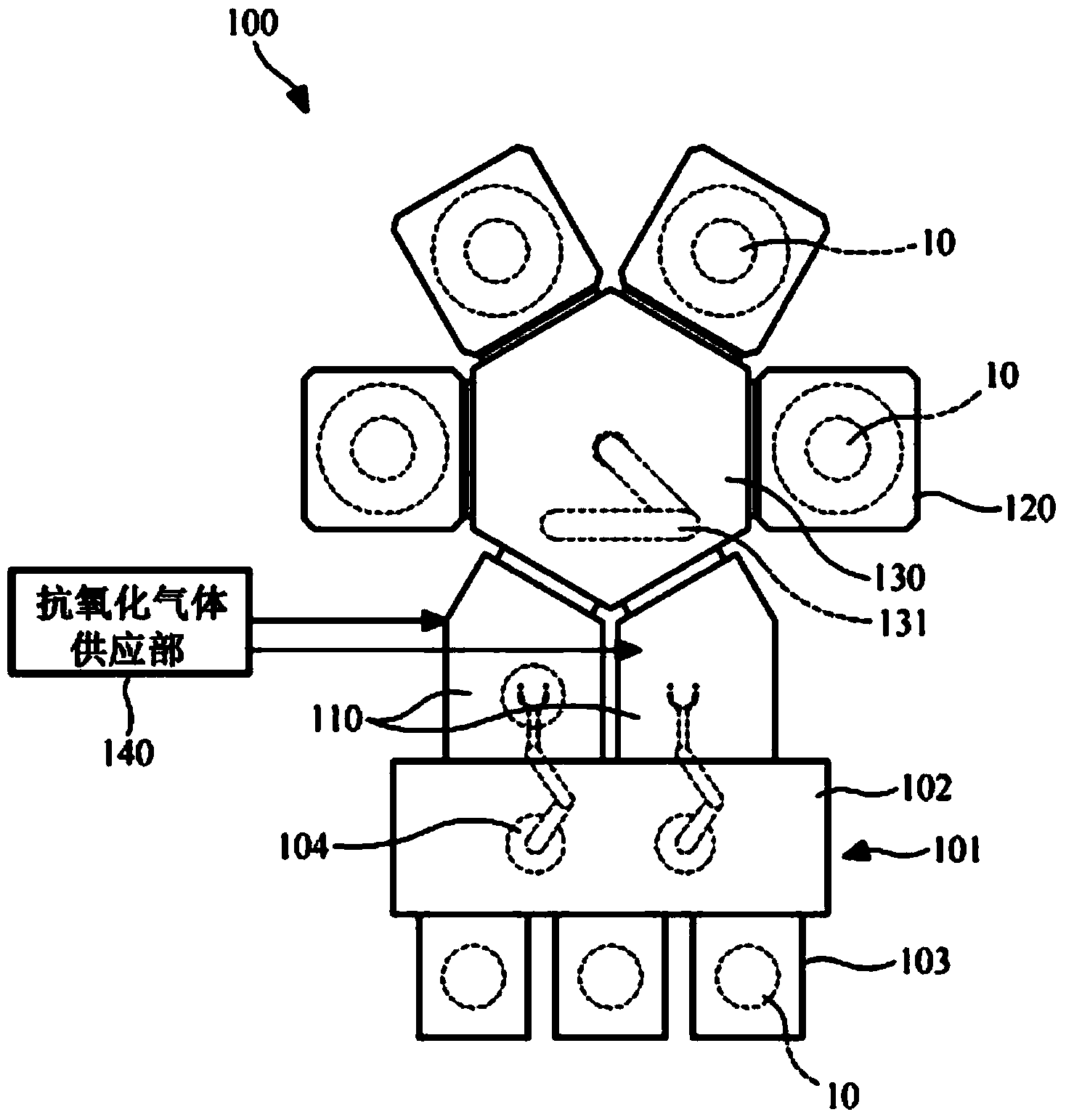
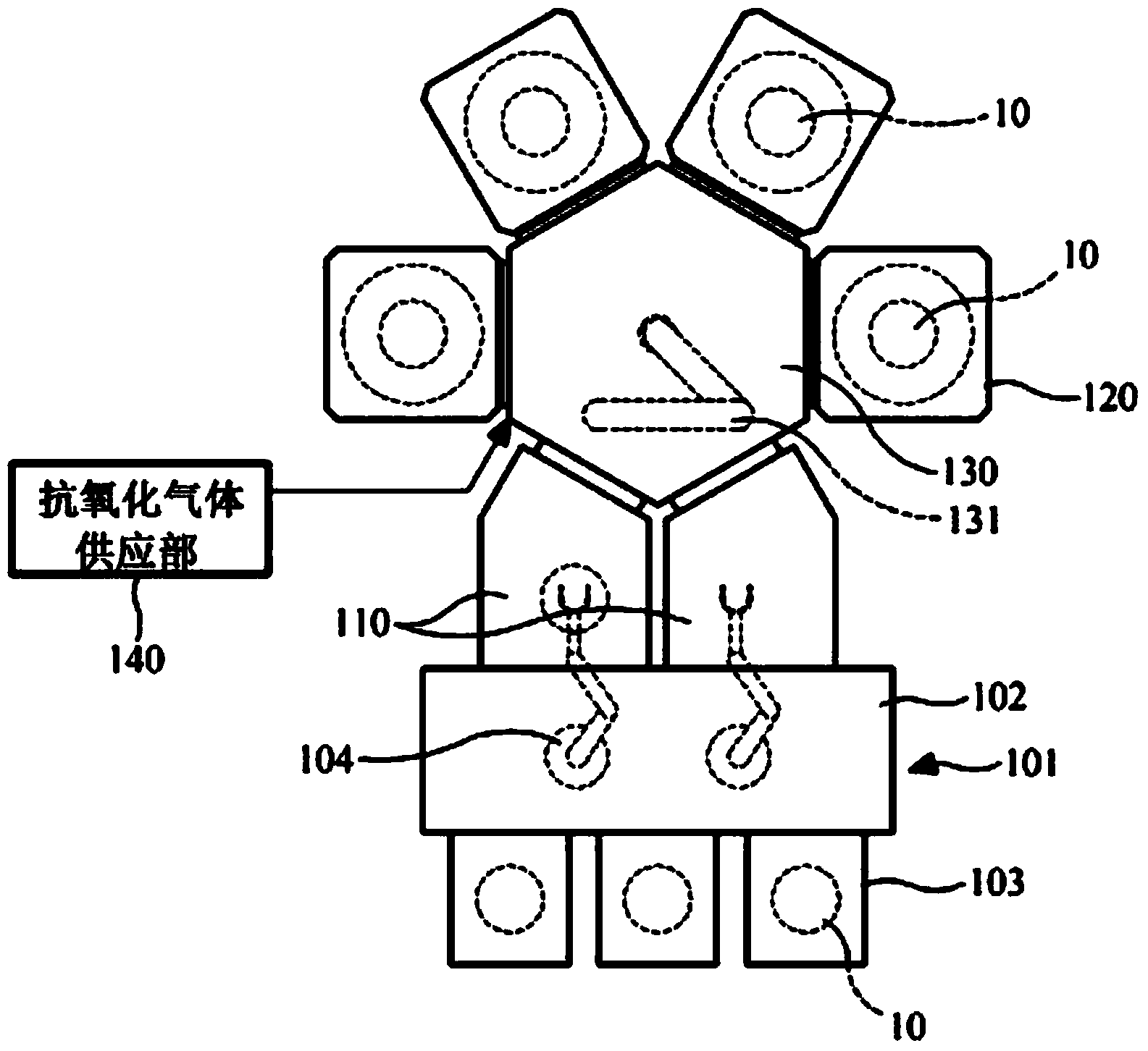
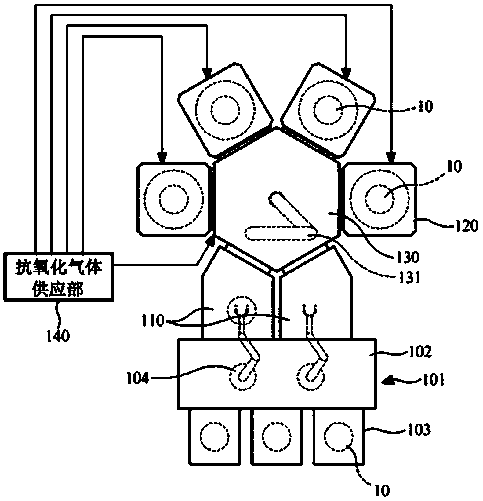
[0020] figure 1 is a configuration diagram of a semiconductor manufacturing apparatus according to a first embodiment of the present invention. refer to figure 1 As shown, the semiconductor manufacturing apparatus 100 includes: a loading chamber 110 ; at least one processing chamber 120 ; a transfer chamber 130 ; and an anti-oxidation gas supply part 140 .

[0021] The carrier chamber 110 accommodates the substrate 10 in a state where the vacuum environment of the processing chamber 120 is kept consistent with the actual state before the substrate 10 such as a wafer is sent into the processing chamber 120 outside the atmospheric pressure environment, or the transfer chamber 130 carries the substrate 10 to the outside. Before sending out, the substrate 10 is housed in a state substantially equal to the external atmospheric pressure environment...


PUM


Abstract

The present invention relates to a semiconductor manufacturing device, which can be applied in a semiconductor metal interconnection process, and a manufacturing method thereof. The semiconductor manufacturing device includes a loadlock chamber, at least one process chamber, a transfer chamber and an oxidation preventing gas supply unit. The process chamber processes an annealing process by receiving a substrate. The transfer chamber transfers the substrate between the loadlock chamber and the process chamber. The oxidation preventing gas supply unit supplies oxidation preventing gas into either the transfer chamber or the loadlock chamber.

Description

technical field [0001] The invention relates to a semiconductor manufacturing device and a manufacturing method, more specifically, a semiconductor manufacturing device and a manufacturing method applicable to semiconductor metal wiring technology. Background technique [0002] Although cheaper and better aluminum is used in the existing semiconductor metal wiring process, copper is used in order to obtain faster signal transmission speed of semiconductor elements. Copper has lower resistivity and higher electromigration resistance characteristics than aluminum. [0003] The wiring process using copper includes the process of forming a contact hole (contact hole) penetrating through the insulating layer after forming a layered conductive layer and insulating layer on the upper substrate surface of a wafer or the like. Afterwards, after the inside of the contact hole is filled with copper, the surface of the filled copper is processed to be smooth by a chemical mechanical po...

Claims


Application Information

Patent Timeline
Patent Type & Authority Applications(China)
IPC IPC(8): H01L21/324
CPCH01L21/67196H01L21/67201H01L21/76883Y10T137/6966Y10T137/0318F17D1/04
Inventor 李起薰柳东浩
Owner WONIK IPS CO LTD
Why Eureka
Try Eureka