Method for observing tsv copper grains

A technology to be observed and applied in the field of microelectronics, it can solve the problems of sample surface damage, difficult control of the reaction time and speed of corrosive liquid and metal, uneven grinding and polishing, etc., achieving high repeatability and strict etching process. controllable effect

Active Publication Date: 2018-02-27
FUDAN UNIV
View PDF5 Cites 0 Cited by
  • Summary
  • Abstract
  • Description
  • Claims
  • Application Information

AI Technical Summary

Problems solved by technology

[0005] The disadvantage of the existing method 1 is: the grinding and polishing of TSV electroplated copper is carried out mechanically by using precision sandpaper and polishing cloth, etc. During the grinding and polishing process, damage to the sample surface, uneven grinding and polishing, and contamination by grinding and polishing debris will occur. problem, affecting follow-up observation
After grinding and polishing, TSV electroplating copper needs to be corroded by corrosive liquid. The corrosion effect is affected by copper metal process, liquid formula, ambient temperature, grinding and polishing roughness, etc. It is difficult to control the reaction time and speed of corrosive liquid and metal. The reproducibility of the effect is poor, and the observation effect is poor
The disadvantage of the existing method 2 is that the price of EBSD equipment is relatively expensive, and the analysis cost is higher than that of scanning electron microscope observation
Moreover, the spatial resolution of EBSD is lower than direct observation by scanning electron microscopy

Method used


Image

  • Method for observing tsv copper grains
  • Method for observing tsv copper grains
  • Method for observing tsv copper grains

Examples


Embodiment Construction

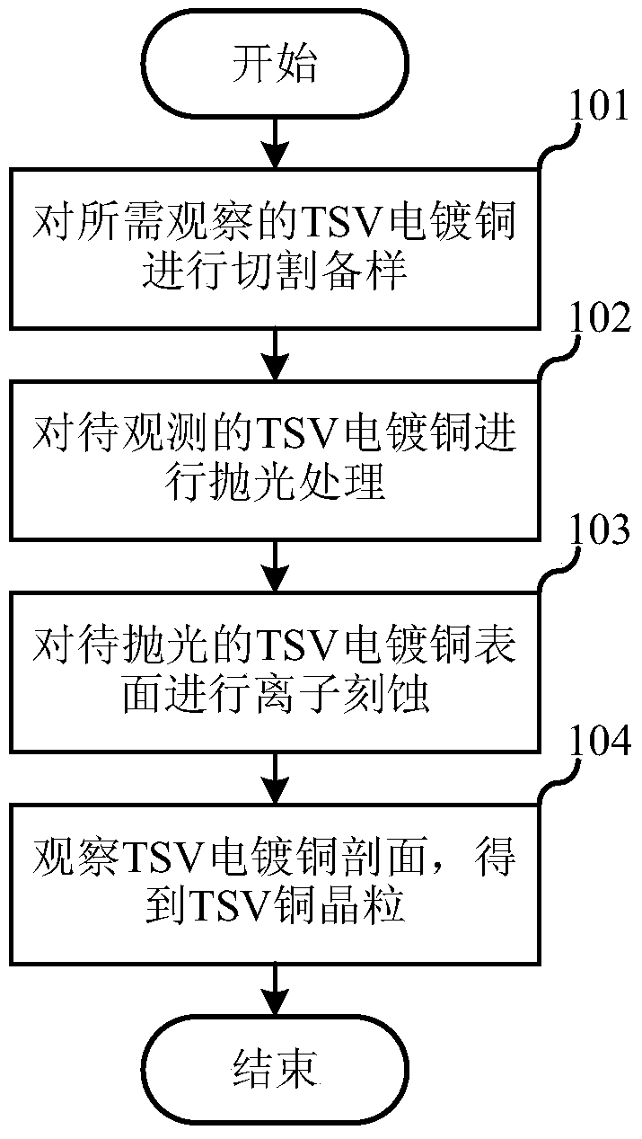
[0031] In order to make the object, technical solution and advantages of the present invention clearer, various embodiments of the present invention will be described in detail below in conjunction with the accompanying drawings. However, those of ordinary skill in the art can understand that, in each implementation manner of the present invention, many technical details are provided for readers to better understand the present application. However, even without these technical details and various changes and modifications based on the following implementation modes, the technical solution claimed in each claim of the present application can be realized.

[0032] The first embodiment of the present invention relates to a method for observing TSV copper grains, the specific process is as follows figure 1 shown.

[0033] In step 101, the TSV electroplated copper to be observed is cut and prepared. Specifically, the TSV electroplated copper to be observed is cut with a slow-spe...


PUM


Abstract

The invention relates to the field of microelectronics and discloses a method for observing TSV copper grains. In the present invention, the electroplated copper to be observed is polished by ion beam; the polished electroplated copper surface is ion-etched by ion beam; the profile of electroplated copper is observed, and finally the grain size and shape of electroplated copper are obtained. The TSV electroplated copper to be observed will not be damaged and contaminated during the polishing process, and the corrosion effect and observation effect during the TSV electroplated copper corrosion process to be observed are also improved. At the same time, the cost of observation equipment is reduced, and the accuracy of observation results is improved. resolution.

Description

technical field [0001] The invention relates to the field of microelectronics, in particular to the observation technology of TSV copper grains. Background technique [0002] High density and high performance are the current development trend of microelectronic packaging, and Through Silicon Vias ("TSV" for short) technology is one of the key packaging technologies to meet this development trend. TSV technology etches micro-holes on the silicon wafer, then fills the micro-holes with copper by electroplating, and then anneals at a high temperature of about 410 degrees to form through-holes through silicon wafer thinning. Combined with the rewiring process to form interconnections and integrate them into the package structure. [0003] In order to analyze the TSV electroplating copper process in the above process, the possible changes of packaged products using through-silicon vias TSV when they experience thermal shock and thermal cycle, and to find evidence for product reli...

Claims


Application Information

Patent Timeline
Patent Type & Authority Patents(China)
IPC IPC(8): G01Q30/20
Inventor 张兆强庞钧文王珺
Owner FUDAN UNIV
Why Eureka
Try Eureka