
OLED (organic light-emitting diode) backboard and manufacturing method for same

A manufacturing method and backplane technology, applied in semiconductor/solid-state device manufacturing, semiconductor devices, electrical components, etc., can solve problems such as the complexity of the OLED backplane manufacturing process, and achieve the effect of avoiding discharge

Active Publication Date: 2014-01-08
BOE TECH GRP CO LTD
View PDF8 Cites 11 Cited by
  • Summary
  • Abstract
  • Description
  • Claims
  • Application Information

AI Technical Summary

Problems solved by technology

[0003] It can be seen that the production process of the existing OLED backplane is relatively complicated

Method used


Image

  • OLED (organic light-emitting diode) backboard and manufacturing method for same
  • OLED (organic light-emitting diode) backboard and manufacturing method for same
  • OLED (organic light-emitting diode) backboard and manufacturing method for same

Examples


Embodiment 1

[0048] Such as Figure 6 As shown, the embodiment of the present invention provides a method for manufacturing an OLED backplane, which can be specifically used to manufacture an OLED backplane for an oxide (Oxide) TFT. The manufacturing method includes:

[0049] Step 101, forming a pattern including TFTs on a substrate;

[0050] This step specifically includes forming a gate, a gate insulating layer, an active layer, an etching stopper layer, a source and a drain.

[0051] Step 102, such as Figure 7 As shown, a passivation layer 3 is formed on the substrate including the above TFT pattern;

[0052] Step 103, forming a color filter 4 on the substrate including the passivation layer 3;

[0053] Specifically, it includes spin-coating the color filter material on the substrate, and sequentially performing exposure, development and annealing.

[0054] Step 104, forming a resin layer 8 on the substrate including the color filter 4;

[0055]Specifically, the resin material is ...

Embodiment 2

[0066] On the basis of Embodiment 1, the embodiment of the present invention provides a method for manufacturing an OLED backplane, such as Figure 11 As shown, among them,

[0067] The above step 104, forming a resin layer on the substrate including the above color filter specifically includes:

[0068] Step 1041, such as Figure 12 As shown, a resin material 81 is deposited on the substrate including the color filter 4;

[0069] Step 1042, such as Figure 8 As shown, the resin material in the pixel electrode area 1 is lightly exposed by halftone exposure, and the resin material in the passivation layer via hole area 2 and its surrounding area is deeply exposed by halftone exposure, finally forming a Figure 13 Resin layer 8 is shown.

[0070] Specifically, the resin material in the pixel electrode region 1 is lightly exposed to thin the resin layer in this region, further ensuring the conductivity of the heavily doped resin layer in this region; similarly, the passivatio...

Embodiment 3

[0076] On the basis of Embodiment 1, the embodiment of the present invention provides a method for manufacturing an OLED backplane, such as Figure 13 As shown, among them,

[0077] The above-mentioned step 104, forming the resin layer 8 on the substrate including the above-mentioned color filter 4 specifically includes:

[0078] Step 1041, depositing a resin material on the substrate including the color filter 4;

[0079] Step 1043: Lightly expose the resin material in the pixel electrode area 1 by halftone exposure, and perform deep exposure on the resin material around the passivation layer via hole area 2 by halftone exposure, and expose the resin material in the passivation layer via hole area 2 Take full exposure.

[0080] Specifically, step 1043 is similar to step 1042 in the second embodiment, the only difference is that in step 1043, the resin material in the passivation layer via area 2 is fully exposed, so that the passivation layer via area 2 has no resin materia...


PUM


Abstract

The invention discloses an OLED (organic light-emitting diode) backboard and a manufacturing method for the same, and relates to the technical field of display. The OLED backboard can be more simply manufactured. The manufacturing method for the OLED backboard comprises the following steps of forming a pattern comprising TFTs (thin film transistors) on a substrate; forming a passivation layer on the substrate with the pattern comprising the TFTs; forming a color film on the substrate comprising the passivation layer; forming a resin layer on the substrate comprising the color film; heavily doping the resin layer in a first area in each sub-pixel on the substrate comprising the resin layer to endow electrical conductivity to the resin layer in the first areas, wherein each first area comprises a passivation layer through hole area, a pixel electrode area and a communicating area between the passivation layer through hole area and the pixel electrode area, and the drains of the TFTs are in the passivation layer through hole areas; sequentially forming an organic luminous layer and an anode on the substrate of which the resin layer in the first areas is heavily doped.

Description

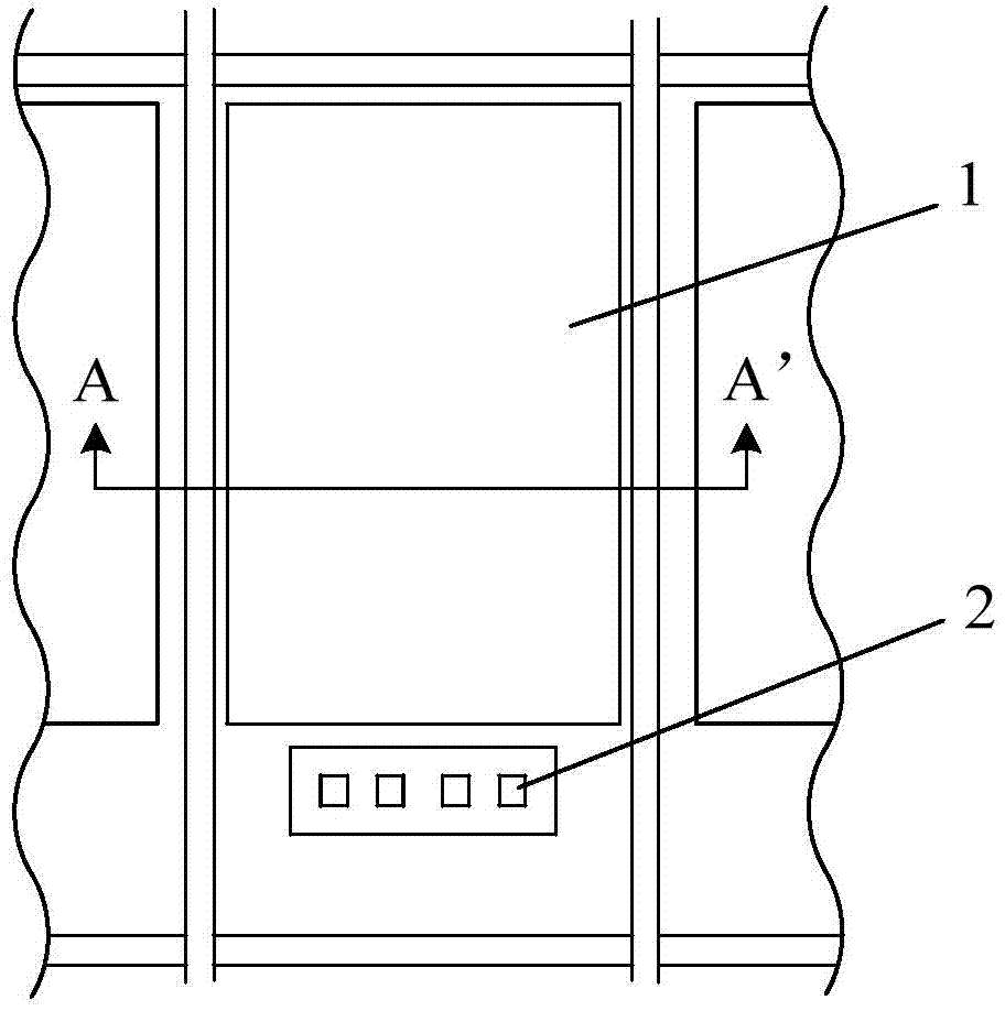
technical field [0001] The present invention relates to the field of display technology, in particular to an organic light-emitting diode (Organic Light-Emitting Diode, OLED) backplane and a manufacturing method thereof. Background technique [0002] The current OLED backplane includes multiple sub-pixels distributed in matrix, such as figure 1 As shown, each sub-pixel includes a pixel electrode region 1 and a passivation layer via hole region 2, and the passivation layer via hole is used to connect the drain of the underlying thin film transistor (Thin Film Transistor, TFT) and the upper pixel electrode. The manufacturing process of the above-mentioned OLED backplane includes: figure 2 As shown, a passivation layer 3 is formed on a substrate with a TFT pattern (not shown in the figure); a color filter 4 is formed on the above-mentioned substrate with a passivation layer 3; as image 3 As shown, a flat layer 5 is formed by depositing resin on the above-mentioned substrate...

Claims


Application Information

Patent Timeline
Patent Type & Authority Applications(China)
IPC IPC(8): H01L21/77H01L51/56H01L27/32
CPCH01L27/1218H01L27/1262H10K59/1201H10K59/124H10K59/122H10K50/81H10K71/00H10K50/84H10K59/12
Inventor 姜春生方婧斐刘威
Owner BOE TECH GRP CO LTD
Learn More